Datasheet Texas Instruments LM2587
| Manufacturer | Texas Instruments |
| Series | LM2587 |
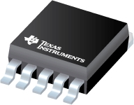
SIMPLE SWITCHERВ® 4V to 40V, 5A Step-Up Wide Vin Flyback Regulator
Datasheets
LM2587 SIMPLE SWITCHER 5A Flyback Regulator datasheet
PDF, 4.2 Mb, Revision: D, File published: Apr 3, 2013
Extract from the document
Prices
Status
| LM2587S-12/NOPB | LM2587S-3.3/NOPB | LM2587S-5.0 | LM2587S-5.0/NOPB | LM2587S-ADJ | LM2587S-ADJ/NOPB | LM2587SX-12/NOPB | LM2587SX-5.0/NOPB | LM2587SX-ADJ | LM2587SX-ADJ/NOPB | LM2587T-12 | LM2587T-12/NOPB | LM2587T-3.3/NOPB | LM2587T-5.0/NOPB | LM2587T-ADJ | LM2587T-ADJ/NOPB | |
|---|---|---|---|---|---|---|---|---|---|---|---|---|---|---|---|---|
| Lifecycle Status | Active (Recommended for new designs) | Active (Recommended for new designs) | NRND (Not recommended for new designs) | Active (Recommended for new designs) | NRND (Not recommended for new designs) | Active (Recommended for new designs) | Active (Recommended for new designs) | Active (Recommended for new designs) | NRND (Not recommended for new designs) | Active (Recommended for new designs) | NRND (Not recommended for new designs) | Active (Recommended for new designs) | Active (Recommended for new designs) | Active (Recommended for new designs) | NRND (Not recommended for new designs) | Active (Recommended for new designs) |
| Manufacture's Sample Availability | Yes | No | Yes | No | Yes | No | Yes | No | No | Yes | Yes | No | Yes | No | Yes | No |
Packaging
| LM2587S-12/NOPB | LM2587S-3.3/NOPB | LM2587S-5.0 | LM2587S-5.0/NOPB | LM2587S-ADJ | LM2587S-ADJ/NOPB | LM2587SX-12/NOPB | LM2587SX-5.0/NOPB | LM2587SX-ADJ | LM2587SX-ADJ/NOPB | LM2587T-12 | LM2587T-12/NOPB | LM2587T-3.3/NOPB | LM2587T-5.0/NOPB | LM2587T-ADJ | LM2587T-ADJ/NOPB | |
|---|---|---|---|---|---|---|---|---|---|---|---|---|---|---|---|---|
| N | 1 | 2 | 3 | 4 | 5 | 6 | 7 | 8 | 9 | 10 | 11 | 12 | 13 | 14 | 15 | 16 |
| Pin | 5 | 5 | 5 | 5 | 5 | 5 | 5 | 5 | 5 | 5 | 5 | 5 | 5 | 5 | 5 | 5 |
| Package Type | KTT | KTT | KTT | KTT | KTT | KTT | KTT | KTT | KTT | KTT | NDH | NDH | NDH | NDH | NDH | NDH |
| Industry STD Term | TO-263 | TO-263 | TO-263 | TO-263 | TO-263 | TO-263 | TO-263 | TO-263 | TO-263 | TO-263 | TO-220 | TO-220 | TO-220 | TO-220 | TO-220 | TO-220 |
| JEDEC Code | R-PSFM-G | R-PSFM-G | R-PSFM-G | R-PSFM-G | R-PSFM-G | R-PSFM-G | R-PSFM-G | R-PSFM-G | R-PSFM-G | R-PSFM-G | R-MSFM-L | R-MSFM-L | R-MSFM-L | R-MSFM-L | R-MSFM-L | R-MSFM-L |
| Package QTY | 45 | 45 | 45 | 45 | 45 | 45 | 500 | 500 | 500 | 500 | 45 | 45 | 45 | 45 | 45 | |
| Carrier | TUBE | TUBE | TUBE | TUBE | TUBE | TUBE | LARGE T&R | LARGE T&R | LARGE T&R | LARGE T&R | TUBE | TUBE | TUBE | TUBE | TUBE | |
| Device Marking | -12 P+ | LM2587S | -5.0 P+ | LM2587S | LM2587S | LM2587S | -12 P+ | LM2587S | -ADJ P+ | -ADJ P+ | LM2587T | -12 P+ | -3.3 P+ | -5.0 P+ | -ADJ P+ | LM2587T |
| Width (mm) | 8.42 | 8.42 | 8.42 | 8.42 | 8.42 | 8.42 | 8.42 | 8.42 | 8.42 | 8.42 | 10.16 | 10.16 | 10.16 | 10.16 | 10.16 | 10.16 |
| Length (mm) | 10.16 | 10.16 | 10.16 | 10.16 | 10.16 | 10.16 | 10.16 | 10.16 | 10.16 | 10.16 | 14.986 | 14.986 | 14.986 | 14.986 | 14.986 | 14.986 |
| Thickness (mm) | 4.58 | 4.58 | 4.58 | 4.58 | 4.58 | 4.58 | 4.58 | 4.58 | 4.58 | 4.58 | 4.572 | 4.572 | 4.572 | 4.572 | 4.572 | 4.572 |
| Pitch (mm) | 1.7 | 1.7 | 1.7 | 1.7 | 1.7 | 1.7 | 1.7 | 1.7 | 1.7 | 1.7 | 1.702 | 1.702 | 1.702 | 1.702 | 1.702 | 1.702 |
| Max Height (mm) | 4.83 | 4.83 | 4.83 | 4.83 | 4.83 | 4.83 | 4.83 | 4.83 | 4.83 | 4.83 | 4.7 | 4.7 | 4.7 | 4.7 | 4.7 | 4.7 |
| Mechanical Data | Download | Download | Download | Download | Download | Download | Download | Download | Download | Download | Download | Download | Download | Download | Download | Download |
Parametrics
| Parameters / Models | LM2587S-12/NOPB | LM2587S-3.3/NOPB | LM2587S-5.0 | LM2587S-5.0/NOPB | LM2587S-ADJ | LM2587S-ADJ/NOPB | LM2587SX-12/NOPB | LM2587SX-5.0/NOPB | LM2587SX-ADJ | LM2587SX-ADJ/NOPB | LM2587T-12 | LM2587T-12/NOPB | LM2587T-3.3/NOPB | LM2587T-5.0/NOPB | LM2587T-ADJ | LM2587T-ADJ/NOPB |
|---|---|---|---|---|---|---|---|---|---|---|---|---|---|---|---|---|
| Approx. Price (US$) | 3.95 | 1ku | |||||||||||||||
| Duty Cycle(Max), % | 98 | 98 | 98 | 98 | 98 | 98 | 98 | 98 | 98 | 98 | 98 | 98 | 98 | 98 | 98 | |
| Duty Cycle(Max)(%) | 98 | |||||||||||||||
| Iq(Typ), mA | 11 | 11 | 11 | 11 | 11 | 11 | 11 | 11 | 11 | 11 | 11 | 11 | 11 | 11 | 11 | |
| Iq(Typ)(mA) | 11 | |||||||||||||||
| Operating Temperature Range, C | -40 to 125 | -40 to 125 | -40 to 125 | -40 to 125 | -40 to 125 | -40 to 125 | -40 to 125 | -40 to 125 | -40 to 125 | -40 to 125 | -40 to 125 | -40 to 125 | -40 to 125 | -40 to 125 | -40 to 125 | |
| Operating Temperature Range(C) | -40 to 125 | |||||||||||||||
| Package Group | DDPAK/TO-263 | DDPAK/TO-263 | DDPAK/TO-263 | DDPAK/TO-263 | DDPAK/TO-263 | DDPAK/TO-263 | DDPAK/TO-263 | DDPAK/TO-263 | DDPAK/TO-263 | DDPAK/TO-263 | TO-220 | TO-220 | TO-220 | TO-220 | TO-220 | TO-220 |
| Rating | Catalog | Catalog | Catalog | Catalog | Catalog | Catalog | Catalog | Catalog | Catalog | Catalog | Catalog | Catalog | Catalog | Catalog | Catalog | Catalog |
| Regulated Outputs | 1 | 1 | 1 | 1 | 1 | 1 | 1 | 1 | 1 | 1 | 1 | 1 | 1 | 1 | 1 | |
| Regulated Outputs(#) | 1 | |||||||||||||||
| Special Features | N/A | N/A | N/A | N/A | N/A | N/A | N/A | N/A | N/A | N/A | N/A | N/A | N/A | N/A | N/A | N/A |
| Switch Current Limit(Min), A | 5 | 5 | 5 | 5 | 5 | 5 | 5 | 5 | 5 | 5 | 5 | 5 | 5 | 5 | 5 | |
| Switch Current Limit(Min)(A) | 5 | |||||||||||||||
| Switch Current Limit(Typ), A | 6.5 | 6.5 | 6.5 | 6.5 | 6.5 | 6.5 | 6.5 | 6.5 | 6.5 | 6.5 | 6.5 | 6.5 | 6.5 | 6.5 | 6.5 | |
| Switch Current Limit(Typ)(A) | 6.5 | |||||||||||||||
| Switching Frequency(Max), kHz | 115 | 115 | 115 | 115 | 115 | 115 | 115 | 115 | 115 | 115 | 115 | 115 | 115 | 115 | 115 | |
| Switching Frequency(Max)(kHz) | 115 | |||||||||||||||
| Switching Frequency(Min), kHz | 85 | 85 | 85 | 85 | 85 | 85 | 85 | 85 | 85 | 85 | 85 | 85 | 85 | 85 | 85 | |
| Switching Frequency(Min)(kHz) | 85 | |||||||||||||||
| Type | Converter | Converter | Converter | Converter | Converter | Converter | Converter | Converter | Converter | Converter | Converter | Converter | Converter | Converter | Converter | Converter |
| Vin(Max), V | 40 | 40 | 40 | 40 | 40 | 40 | 40 | 40 | 40 | 40 | 40 | 40 | 40 | 40 | 40 | |
| Vin(Max)(V) | 40 | |||||||||||||||
| Vin(Min), V | 4 | 4 | 4 | 4 | 4 | 4 | 4 | 4 | 4 | 4 | 4 | 4 | 4 | 4 | 4 | |
| Vin(Min)(V) | 4 | |||||||||||||||
| Vout(Max), V | 60 | 60 | 60 | 60 | 60 | 60 | 60 | 60 | 60 | 60 | 60 | 60 | 60 | 60 | 60 | |
| Vout(Max)(V) | 60 | |||||||||||||||
| Vout(Min), V | 1.23 | 1.23 | 1.23 | 1.23 | 1.23 | 1.23 | 1.23 | 1.23 | 1.23 | 1.23 | 1.23 | 1.23 | 1.23 | 1.23 | 1.23 | |
| Vout(Min)(V) | 1.23 |
Eco Plan
| LM2587S-12/NOPB | LM2587S-3.3/NOPB | LM2587S-5.0 | LM2587S-5.0/NOPB | LM2587S-ADJ | LM2587S-ADJ/NOPB | LM2587SX-12/NOPB | LM2587SX-5.0/NOPB | LM2587SX-ADJ | LM2587SX-ADJ/NOPB | LM2587T-12 | LM2587T-12/NOPB | LM2587T-3.3/NOPB | LM2587T-5.0/NOPB | LM2587T-ADJ | LM2587T-ADJ/NOPB | |
|---|---|---|---|---|---|---|---|---|---|---|---|---|---|---|---|---|
| RoHS | Compliant | Compliant | See ti.com | Compliant | See ti.com | Compliant | Compliant | Compliant | See ti.com | Compliant | Not Compliant | Compliant | Compliant | Compliant | See ti.com | Compliant |
| Pb Free | Yes | Yes | Yes | Yes | Yes | Yes | Yes | Yes | Yes | Yes | Yes | No |
Application Notes
- Softstart Using Constant Current Constant Voltage ApproachPDF, 337 Kb, File published: Jul 24, 2015
In many systems backup power is provided either by batteries or simply by a large value capacitor. Inthese applications the capacitor would only provide the current when the primary power source fails.Further, these applications are usually for light load currents. During normal operation the backupcapacitors are kept charged up by a DC/DC converter. The challenge involved in an application - AN-643 EMI/RFI Board Design (Rev. B)PDF, 742 Kb, Revision: B, File published: May 3, 2004
Application Note 643 EMI/RFI Board Design - Working With Boost ConvertersPDF, 159 Kb, File published: Jun 15, 2015
This brief note highlights some of the more common pitfalls when using boost regulators. These includemaximum achievable output current and voltage, short circuit behavior and basic layout issues. It isassumed that the reader is familiar with the basic operation of a boost regulator. - Input and Output Capacitor SelectionPDF, 219 Kb, File published: Sep 19, 2005
- Basic Calculation of a Boost Converter's Power Stage (Rev. C)PDF, 186 Kb, Revision: C, File published: Jan 8, 2014
This application note gives the equations to calculate the power stage of a boost converter built with an IC with integrated switch and operating in continuous conduction mode. It is not intended to give details on the functionality of a boost converter (see Reference 1) or how to compensate a converter. See the references at the end of this document if more detail is needed. - AN-2155 Layout Tips for EMI Reduction in DC/ DC Converters (Rev. A)PDF, 3.6 Mb, Revision: A, File published: Apr 23, 2013
This application note will explore how the layout of your DC/DC power supply can significantly affect theamount of EMI that it produces. It will discuss several variations of a layout analyze the results andprovide answers to some common EMI questions such whether or not to use a shielded inductor. - AN-1566 Techniques for Thermal Analysis of Switching Power Supply Designs (Rev. A)PDF, 1.4 Mb, Revision: A, File published: Apr 23, 2013
This application note provides thermal power analysis techniques for analyzing the power IC. - AN-1889 How to Measure the Loop Transfer Function of Power Supplies (Rev. A)PDF, 2.7 Mb, Revision: A, File published: Apr 23, 2013
This application report shows how to measure the critical points of a bode plot with only an audiogenerator (or simple signal generator) and an oscilloscope. The method is explained in an easy to followstep-by-step manner so that a power supply designer can start performing these measurements in a shortamount of time. - Semiconductor and IC Package Thermal Metrics (Rev. C)PDF, 201 Kb, Revision: C, File published: Apr 19, 2016
- Dual LM2587 Boost Converter, -5V input to +5V, 2A OutputPDF, 48 Kb, File published: Mar 21, 2007
- Negative Input to Positive Output made SIMPLEPDF, 645 Kb, File published: Jul 9, 2015
There can be quite a few applications that require a conversion from a negative input voltage to a positive output voltage. This design space along with being limited is not well explored. There are a few ways to go about doing it. In this application note we will go over the use of an integrated boost regulator to convert a negative input voltage to a positive output voltage. - Inverted SEPIC Made SIMPLEPDF, 408 Kb, File published: Jul 31, 2015
There can be quite a few applications that require a conversion from a negative input voltage to a negativeoutput voltage and there are a few ways to go about doing it. The telecom industry is one such examplewhere the rails are usually negative. This design space along with being limited is not well explored. In thisapplication note we will go over the use of an integrated boost regulator i - AN-1095 Design of Isolated Converters Using Simple Switchers (Rev. B)PDF, 631 Kb, Revision: B, File published: Apr 23, 2013
This application note discusses the design of isolated converters using simple switchers. - AN-1082 Adjust or Synchronize LM2586/88 Switching Frequency (Rev. B)PDF, 69 Kb, Revision: B, File published: Apr 23, 2013
Switching frequency is a very important parameter in switching power converters. As the switchingfrequency increases, the physical size of magnetic elements and other components in the circuit reducesignificantly. Switching frequency also plays a great role in control loop gain and compensation design.Switching frequency determines the maximum allowable bandwidth of the control loop. Switchi - AN-1149 Layout Guidelines for Switching Power Supplies (Rev. C)PDF, 82 Kb, Revision: C, File published: Apr 23, 2013
When designing a high frequency switching regulated power supply layout is very important. Using agood layout can solve many problems associated with these types of supplies. The problems due to a badlayout are often seen at high current levels and are usually more obvious at large input to output voltagedifferentials. Some of the main problems are loss of regulation at high output current - Understanding Boost Power Stages In Switchmode Power SuppliesPDF, 149 Kb, File published: Mar 4, 1999
A switching power supply consists of the power stage and the control circuit. The power stage performs the basic power conversion from the input voltage to the output voltage and includes switches and the output filter. This report addresses the boost power stage only and does not cover control circuits. The report includes detailed steady-stage and small-signal analysis of the boost power stage o - Increasing Available Load Power in an LM2587 Boost Regulator (by Paralleling)PDF, 66 Kb, File published: Mar 21, 2007
- AN-1229 SIMPLE SWITCHER PCB Layout Guidelines (Rev. C)PDF, 374 Kb, Revision: C, File published: Apr 23, 2013
This application report provides SIMPLE SWITCHER™ PCB layout guidelines. - AN-2162 Simple Success With Conducted EMI From DC-DC Converters (Rev. C)PDF, 2.5 Mb, Revision: C, File published: Apr 24, 2013
Electromagnetic Interference (EMI) is an unwanted effect between two electrical systems as a result ofeither electromagnetic radiation or electromagnetic conduction. EMI is the major adverse effect caused bythe application of switch-mode power supplies (SMPS). In switching power supplies EMI noise isunavoidable due to the switching actions of the semiconductor devices and resulting disconti - AN-1520 A Guide to Board Layout for Best Thermal Resistance for Exposed Packages (Rev. B)PDF, 9.2 Mb, Revision: B, File published: Apr 23, 2013
This thermal application report provides guidelines for the optimal board layout to achieve the best thermalresistance for exposed packages. The thermal resistance between junction-to-ambient (ОёJA) is highlydependent on the PCB (Printed Circuit Board) design factors. This becomes more critical for packageshaving very low thermal resistance between junction-to-case such as exposed pad TSSOP
Model Line
Series: LM2587 (16)
Manufacturer's Classification
- Semiconductors> Power Management> Non-isolated DC/DC Switching Regulator> Step-Up (Boost)> Boost Converter (Integrated Switch)
