With RMS Additive Phase Jitter of Sub-50 fsec, the new Buffers Deliver Best-in-Class Performance in an Extremely Small 2 Millimeter-by-2 Millimeter Package
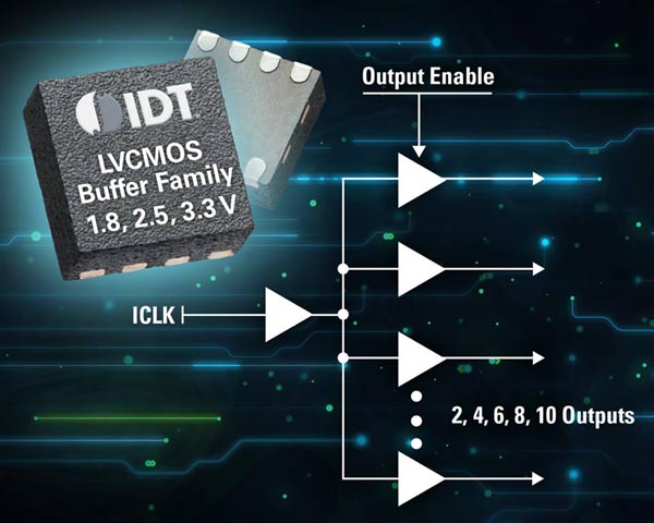
Integrated Device Technology (IDT) introduced a new family of clock buffers that deliver best-in-class jitter performance in a compact package. The 5PB11xx family of LVCMOS fanout buffers provides low-jitter metrics of sub-50 fsec RMS additive phase jitter (12 kHz to 20 MHz), offering system designers greater jitter margin than competitive products to help them meet system clock requirements. The small die size enables the chip to fit within a DFN 8-pin package as small as 2 by 2 millimeters.
The buffers are ideal for high-end consumer, industrial, data communications, telecommunications and computing applications where both timing budget and board space are at a premium.
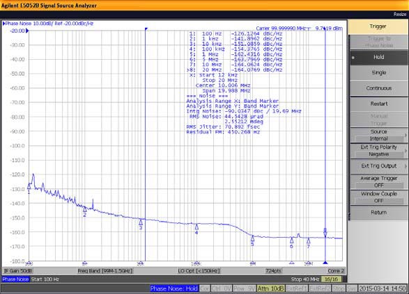 |
| 5PB11xx Output Phase Noise 70.9 fs (12 kHz to 20 MHz). |
The new buffers are available with 2, 4, 6, 8 and 10 LVCMOS outputs and can support 1.8 V, 2.5 V and 3.3 V power supplies and outputs. They have a low output skew of 50 psec with only 14 mA core current consumption. All the devices in the new buffer family are characterized at an extended temperature of –40 °C to 105 °C enabling the new buffers to meet the requirements of automotive infotainment applications as well.
Along with the 5PB11xx family, IDT has introduced a 551S and 553S 1:4 LVCMOS fanout buffer series with sub-50 fsec additive jitter in industry-standard 551 and 553 footprints. These devices are also available in 2-by-2-millimeter DFN 8-pin packages and support 1.8 V, 2.5 V and 3.3 V power supplies and outputs.
Pricing and Availability
The new cost-competitive buffers start at $0.8 for 1K pricing and are available within a short lead time.
