Risky alternatives could be postponed if current methods can be modified to last longer
IBM researchers announced they have found a way to extend a key chip-manufacturing process to generate smaller chip circuits, potentially postponing the semiconductor industry's high-risk conversion to an extremely expensive alternative.
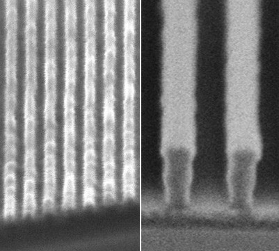
IBM scientists have created the smallest, high-quality line patterns ever made using deep-ultraviolet (DUV, 193-nanometer) optical lithography – a technology currently used to essentially “print” circuits on chips. The distinct and uniformly spaced ridges are only 29.9 nanometers wide (a nanometer is a billionth of a meter). This is less than one-third the size of the 90-nanometer features now in mass production and below the 32 nanometers that industry consensus held as the limit for optical lithography techniques.

Pictured on the left is the record-small array of 29.9-nanometer-wide lines and equally sized spaces created by IBM scientists (at its Almaden Research Center in San Jose, California) using a variation of optical lithography. These lines are less than one-third the size of the 90-nanometer features (example at right, same magnification) now in mass production by the microchip industry. They are also smaller than the 32-nanometer size that industry consensus held was the limit for optical lithography techniques. By creating such small features using optical lithography, the IBM researchers have shown the industry a possible route for extending the current manufacturing processes to generate ever-smaller chip circuits. Such an extension may also postpone a high-risk conversion to an extremely expensive alternative.
For decades, the semiconductor industry has relied on continually shrinking circuits to drive increases in the performance and function of chips and the products that use them. But as chip features now approach the fundamental scale limits of individual atoms and molecules, the future of this trend of relentless improvement, known as Moore's Law, is being threatened. IBM’s new result indicates that a "high-index immersion" variant of DUV lithography may provide a path for extending Moore’s Law further, thus buying the industry time.
Technical details
Microelectronic chips are made by a process called photolithography, which is similar in concept to silk-screening – except it uses light instead of paint or ink. Photolithography transfers the various circuit design patterns onto a silicon wafer by projecting a uniform beam of laser light through a shadow mask and then focusing it onto a photosensitive "photoresist" material that coats the silicon wafer. Subsequent development, etching, and materials deposition steps form the circuit features. Making a typical computer processor or memory chip may require dozens of photolithography cycles.
Over the years, the industry has created smaller circuit features – which typically lead to smaller, faster and cheaper electronics -- by using ever-shorter wavelengths of light, stronger lenses and – most recently – inserting between the final lens and the silicon wafer a liquid, currently water, that enables even finer resolution.
Until now, it was not known if the industry could continue to adapt this optical immersion technique to produce sharp features smaller than 32 nanometers. New materials required to make such small features were thought to be incompatible with each other or capable of yielding only indistinct, blurred patterns. As a result, in recent years contingency plans are being explored for switching sometime in the future to a radically different but much more expensive – and still unproven -- manufacturing method that uses soft-x-rays (also known as EUV, for extreme ultraviolet light) and exotic mirrors rather than laser light and lenses.
As part of its efforts to extend current optical lithography techniques, IBM developed an industry-leading interference immersion lithography test apparatus, called NEMO. IBM's NEMO tool uses two intersecting laser beams to create light-and-dark interference patterns with spacings closer than can be made with current chip-making apparatus. As a result, NEMO is ideal for researching, testing and optimizing the various high-index fluids and photoresists being considered for use in those future DUV systems that would create such fine features. Now that IBM's new result shows a path for extending optical lithography, high-index lens materials must be developed to enable its commercial viability.
When light passes through a transparent material, it slows down in proportion to the material's "refractive index." Light passing through a higher-index material has a shorter wavelength and can thus be focused more tightly. Resolution in immersion lithography is limited by the lowest refractive index of the final lens, fluid and photoresist materials. In IBM's NEMO experiments, the lens and fluid had indices of about 1.6, and the photoresist's index of refraction was 1.7. Future research is aimed at developing lens, fluid and photoresist materials with indices of refraction of 1.9, which would enable even smaller features to be imaged.
