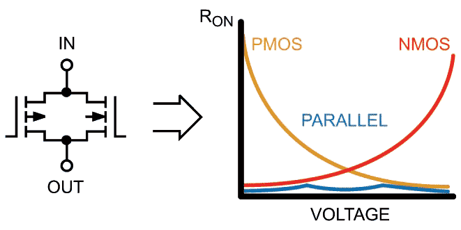
Bandwidth
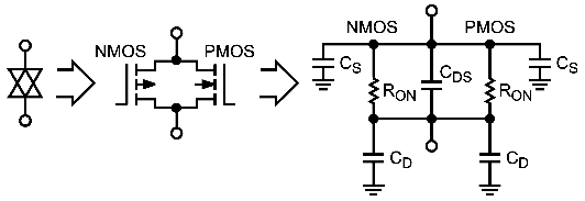
Figure 7 shows the parasitic components that affect the ac performance of CMOS switches.
CDS = drain-source capacitance;
CD = drain-gate + drain-bulk capacitance;
CS = source-gate + source-bulk capacitance.
 |
|
| Figure 7. | CMOS switch model. |
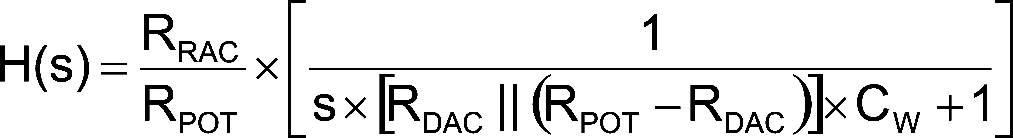
The transfer relationship is defined in the equation below, where these assumptions have been applied:
- Source impedance is 0 Ω
- No external load contribution
- No contribution from CDS
- RLSB << RMSB
![]()
where:
RDAC is the resistance setting
RPOT is the end-to-end resistance
CDLSB is the total drain-gate + drain-bulk capacitance in the LSB segment
CSLSB is the total source-gate + source-bulk capacitance in the LSB segment
CDMSB is the drain-gate + drain-bulk capacitance in the MSB switch
CSMSB is the source-gate + source-bulk capacitance in the MSB switch
moff is the number of off switches in the signal MSB path
mon is the number of on switches in the signal MSB path
The transfer equation has many factors and is somewhat code-dependent, so the following further assumptions are used to simplify the equation
CDMSB + CSMSB = CDSMSB
CDLSB + CSLSB >> CDSMSB
(CDLSB + CSLSB) = CW (specified in the data sheet)
The CDS contribution adds a zero in the transfer equation, but since this occurs typically at much higher frequency than the pole, an RC low-pass filter is the dominant response. A good approximation of the simplified equation is:
and the bandwidth (BW) is defined as:
![]()
where CL is the load capacitance.
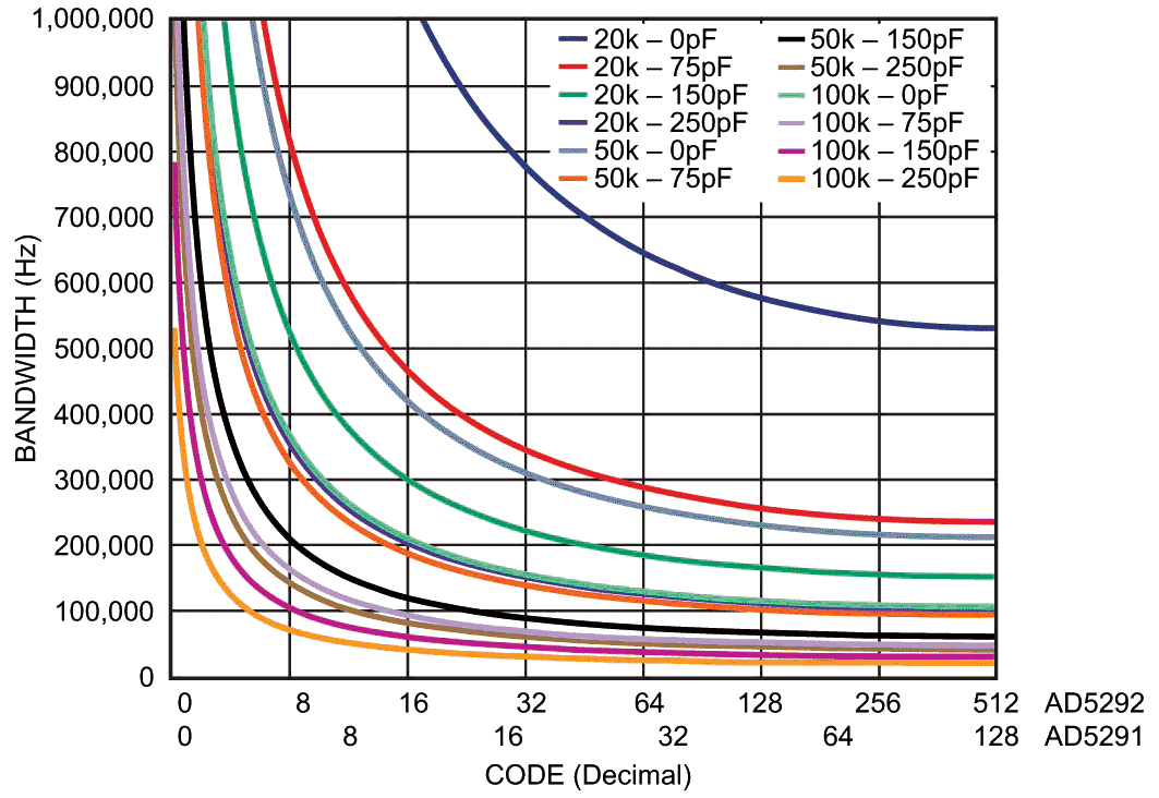
The BW is code dependent, and the worst case is when the code is at half scale, a digital value of 29 = 512 for the AD5292 and 27 = 128 for the AD5291 (see Appendix). Figure 8 shows the low-pass filtering effect as a function of code for various nominal resistance and load capacitance values.
 |
|
| Figure 8. | Maximum bandwidth vs. load capacitance for various resistance values. |
The parasitic track capacitance of the PC board should be taken into account, otherwise the maximum BW will be lower than expected; the track capacitance can be calculated straightforwardly as
![]()
where
εR is the dielectric constant of the board material
A is the track area (cm2)
d is the distance between layers (cm)
For example, assuming FR4 board material with two signal layers and power/ground planes, εR = 4, track length = 3 cm, width = 1.2 mm, and distance between layers = 0.3 mm; the total track capacitance is about 4 pF.
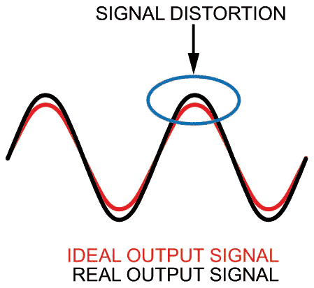
Distortion
The THD is used to quantify the nonlinearity of the device as an attenuator. This nonlinearity is due to the internal switches and their RON variation with voltage. An exaggerated example of amplitude distortion is shown in Figure 9.
 |
|
| Figure 9. | Distortion. |
The RON of a switch is quite small when compared with the resistance of a single internal passive resistor, and its variation over the signal range is even smaller. Figure 10 shows a typical on-resistance characteristic.
 |
|
| Figure 10. | CMOS resistance. |
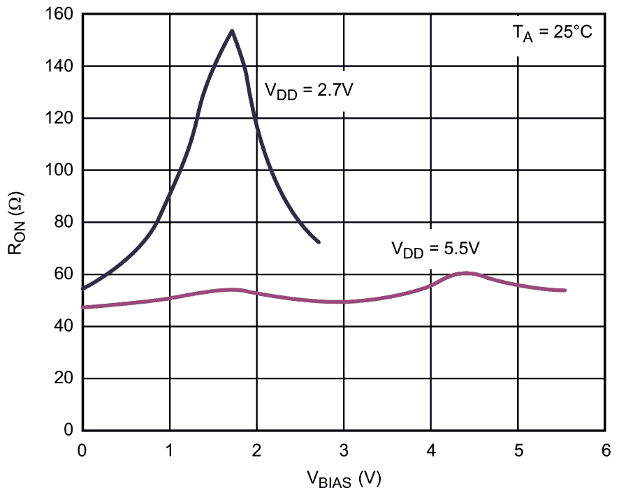
The resistance curve does depend on the supply voltage rails; the internal switches have the lowest RON variation at maximum supply voltage. If the supply voltage is decreased, the RON variation, and hence the nonlinearity, increases. Figure 11 compares RON variation at two supply levels for a low-voltage digiPOT.
The THD depends on multiple factors and is thus hard to quantify, but assuming a 10% variation in RON, the following equation can be used as a rough approximation:
As a general rule, the higher the nominal digiPOT resistance (RPOT), the better the THD, as the denominator is larger.
 |
|
| Figure 11. | Switch resistance variation vs. supply voltage. |
Trade-Offs
Distortion and bandwidth both decrease with increased RPOT, so it is not possible to improve one specification without penalizing the other. So the circuit designer must choose an appropriate balance. This is also true at the device design level, since the IC designer must balance the parameters in the design equations:
![]()
![]()
where
COX is the oxide capacitance
μ is the mobility constant of the electron (NMOS) or hole (PMOS)
W is the width
L is the length
Biasing
From the practical point of view one must make the best of these specifications. When the digiPOT is used to attenuate an ac signal with capacitive coupling, the lowest distortion is achieved if the signal is biased to the mid-value of the power supply. This means that the switches are working on the most linear portion of the resistance characteristic.
One approach is to use a dual supply and simply ground the potentiometer to the power-supply common. The signal can then have a positive-negative swing. Another way, if a single supply is required, or the particular digiPOT doesn’t support dual supply, is to add an offset voltage of VDD/2 to the ac signal. This offset voltage must be added at both resistor terminals, as shown in Figure 12.
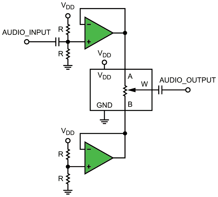 |
|
| Figure 12. | Single-supply ac signal conditioning. |
If a signal amplifier is required, an inverting amplifier, with a dual supply, as shown in Figure 13, is preferred over the noninverting amplifier for two reasons:
- Provides better THD performance because the virtual ground at the inverting pin will center the switch resistance in the middle of the voltage range.
- As the inverting pin is at virtual ground, the wiper capacitance, CDLSB, is almost canceled to obtain a small increase in bandwidth (but one must pay attention to circuit stability).
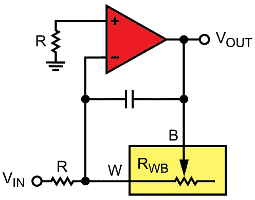 |
|
| Figure 13. | Adjustable amplification using a digiPOT with an inverting amplifier. |
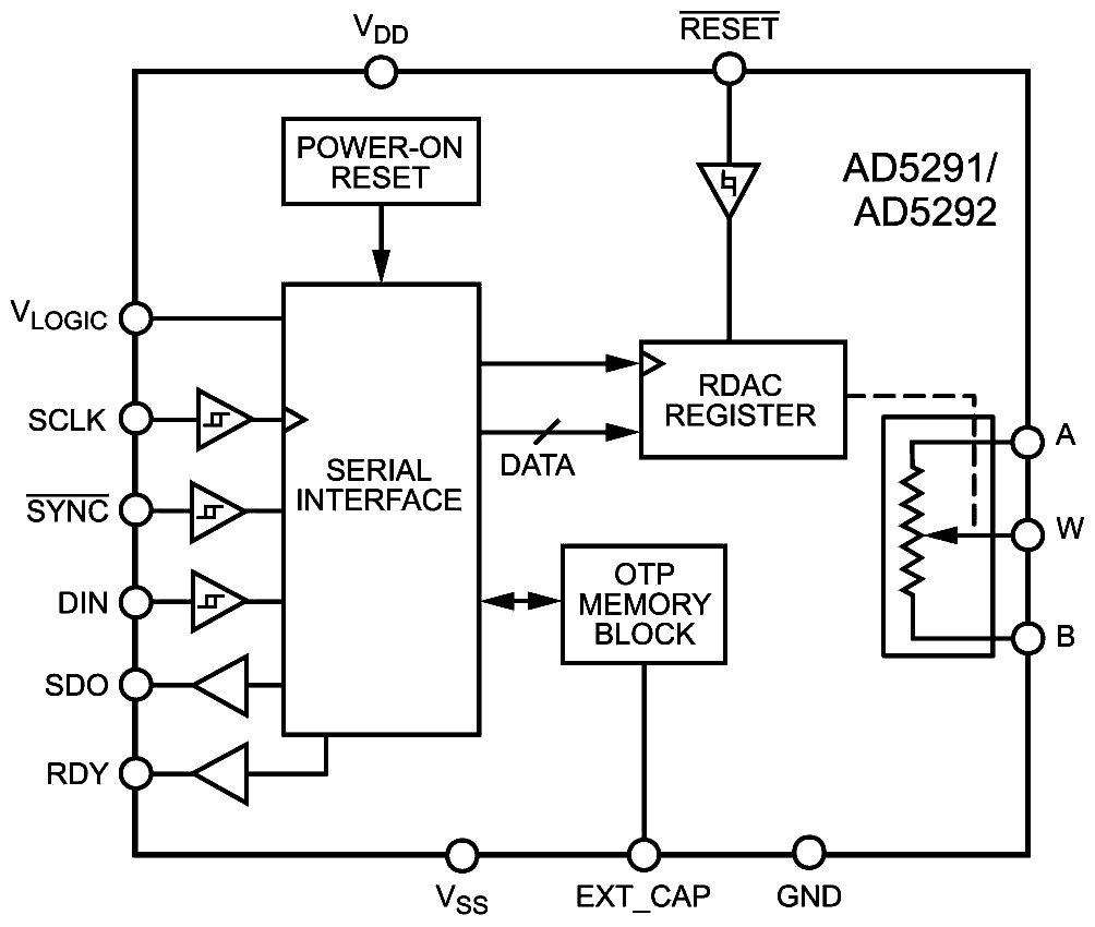
APPENDIX—ABOUT THE AD5291/AD5292
 |
|
| Figure 14. | AD5291/AD5292 functional block diagram. |
The AD5291/AD5292 digital potentiometers, shown in Figure 14, feature 256-/1024-position resolution. End-to-end resistance options of 20 kΩ, 50 kΩ, and 100 kΩ are available, with better than 1% tolerance—and temperature coefficients of 35 ppm/°C in rheostat mode and 5 ppm/°C (ratio) in divider mode. The devices perform the same electronic adjustment function as mechanical potentiometers, but are smaller and more reliable. Their wiper position can be adjusted via an SPI-compatible interface. Unlimited adjustments can be made before blowing a fuse to fix the wiper position, a process analogous to putting epoxy on a mechanical trimmer. This process can be repeated up to 20 times (“removing the epoxy”). Operating on a single 9-V to 33-V supply or dual ±9-V to ±16.5-V supplies, the AD5291/AD5292 dissipate 8 μW. Available in 14-lead TSSOP packages, they are specified from –40°C to +105°C.
