Edward Ong, Power Integrations
New Electronics
With standby power consumption representing a significant proportion of electricity consumed around the world, standards for no load performance are tightening. For example, the European Commission's Energy-related Products (ErP) Directive Tier 1, which permitted a no load consumption of 0.5 W for products manufactured in 2010, was tightened in 2011 to 300 mW for adapters with an output less than 51 W.
When energy use standards were initially developed, targets were set at the levels achievable using the best technology available at the time. However, recent developments in switch mode power supply ic technology have enabled standby consumption levels much lower than the mandated requirements.
Zero power
IEC 62301 describes zero standby as 'power dissipation below 5 mW'. Achieving zero watt standby power is therefore realistic and achievable.
To meet the zero standby challenge, each section of the power supply must be optimised, saving a few mW with each adjustment. Two areas of power supply performance to consider are consumption under very low load and consumption under no load.
Low load or standby conditions apply when the power supply is still active and must provide a regulated output. No load typically relates to power adapters or chargers when the load is disconnected, but the adapter is left plugged into the mains. These conditions present different challenges.
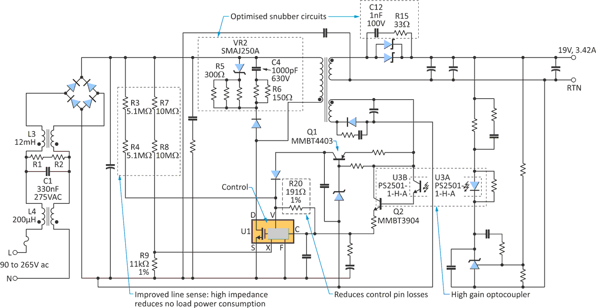
The goal of the 65 W power supply shown in Figure 1 was to produce a very compact notebook adapter that operates at high efficiency, has a low parts count, provides excellent load response, has latching overvoltage protection and derates the MOSFET switch to 80% for ultimate reliability. The design provides a 3.42 A, 19 V output at an efficiency of more than 86%, yet achieves a no load consumption of <90mW at 230 V ac.
 |
|
| Figure 1. | An optimised 65W switch mode power supply. |
It uses a TOPSwitch-JX controller and driver IC (U1) from Power Integrations. TOPSwitch-JX devices maintain virtually constant efficiency across a wide load range without using special operating modes. However, when the goal is to achieve sub 100 mW no load consumption, every opportunity to save power must be exploited. Major contributions can be made at the line sensing network and input filter, although there are other opportunities.
Line sense resistors (R3 and R4) provide a line condition input to U1 and the required minimum bias current of 25 µA. While the standard value for these resistors is 4 MOhm, this results in a power drain of 30 mW at 230 V ac. By increasing line sensing resistance to 10.2 MOhm, this power dissipation is reduced to 16 mW. This required a further resistor to provide additional bias current and maintain the same line undervoltage threshold.
Resistors R7, R8, and R9 reduce the external current limit of U1 as the line voltage increases. This allows the supply to limit the output power to <100 VA at high line, while still delivering the rated output power at low line, and to provide a nearly constant output over load power level with changing line voltages.
The clamp network limits the peak drain voltage spike caused by leakage inductance to less than the saturated drain-source breakdown voltage rating of the TOPSwitch-JX's MOSFET. Under light or no load conditions, the leakage inductance energy and switching frequency are lower. In a standard RCD clamp, capacitor C4 is discharged and recharged each cycle, wasting a significant amount of energy. The RZCD arrangement solves this by preventing the voltage across the capacitor discharging below a minimum value (defined by VR2) and therefore minimising clamp dissipation.
High current rating, low Vf Schottky rectifier diodes were selected to reduce diode loss and improve efficiency. The snubber network (C12, R15) dampens ringing across the diodes and reduces high frequency conducted and radiated noise.
To minimise the dissipation of the secondary side feedback circuit, a high gain optocoupler was selected, with Q2 added to form a Darlington connection with U3B. This reduced the feedback current on the secondary to 1 mA.
Eliminating power waste
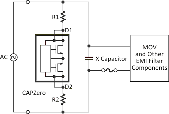
Filtering at the ac input is provided by common mode inductors L3 and L4, an X class capacitor C1 provides differential filtering and resistors R1 and R2 provide a path for C1 to discharge. These resistors are undesirable because they dissipate 12 mW at 230 V ac.
Subsequent to the supply's design, PI introduced the CAPZero ic that eliminates this source of wasted power. Each CAPZero integrates a loss of ac detector and back to back MOSFETs (Figure 2). When the ac input voltage is present, CAPZero remains off, blocking current flow in the discharge path and eliminating power losses. When the ac is removed, it turns on, switching in the resistors and allowing discharge of the input filter capacitance.
 |
|
| Figure 2. | CAPZero typical application – not a s implified circuit. |
Line sensing
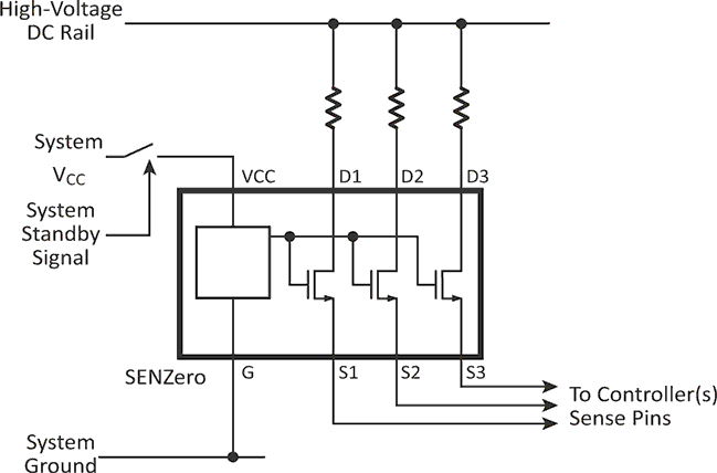
In the design example, the line sense resistor values have been increased as far as possible to minimise dissipation. However, they still draw significant energy from the mains, regardless of whether U1 is operational or static. In high power applications, there may be several paths between high voltage rails; for example, feed forward or feedback signal paths connected to boost controllers in power factor correction (PFC) systems. The power drain through these paths can be eliminated with the use of a
SENZero device
SENZero comprises two or three 650 V MOSFETs with internal gate drive and protection circuitry. The control circuitry provides gate drive to the MOSFETs in response to the voltage at the Vcc pin. In a typical application, the MOSFETs are connected in series with resistor paths running from the high voltage dc rail to 0 V or to the controller (Figure 3). SENZero has a typical on state resistance of 500 Ohm at room temperature, a small percentage of the high value resistors typically used.
 |
|
| Figure 3. | Typical application SENZero. |
When the system enters standby, Vcc falls and gate drive is removed from the MOSFETs. The MOSFETs then switch to high impedance and isolate the current paths from the high voltage dc rail. Power losses are consequently reduced to less than 500 µW per channel.
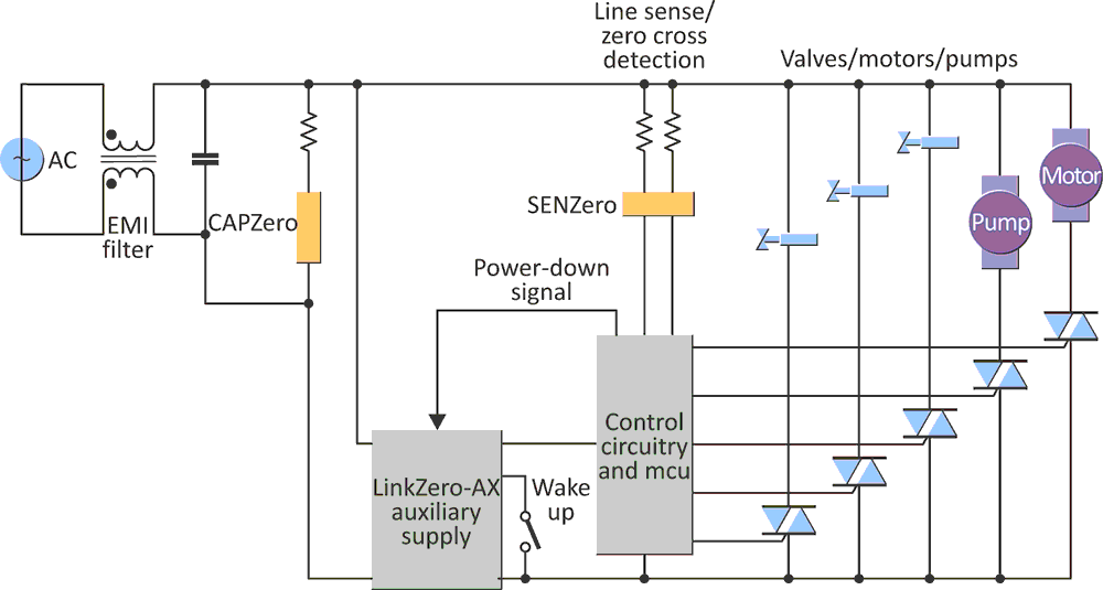
Figure 4 illustrates how ultra low standby power could be implemented in a white goods application – in this case, a washing machine.
 |
|
| Figure 4. | Washing machine application providing zero standby power drain. |
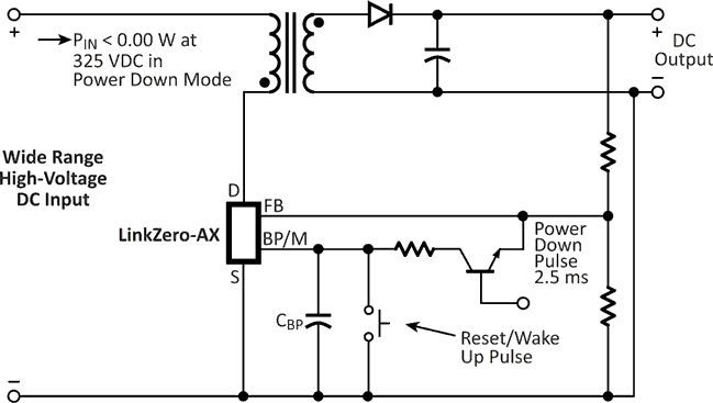
The system is put into standby by a power down pulse from the control circuitry. LinkZero-AX (Figure 5) stops switching and remains in a quiescent state. A CAPZero device at the ac mains input isolates the X capacitor discharge resistor. A SENZero device isolates the line sense and zero crossing resistors from the power line, which still has ac mains applied. When LinkZero-AX is woken up, it starts switching and brings up the regulated Vcc. The Vcc voltage applied to SENZero triggers it to switch on the two internal MOSFETs. These feed the line sense and zero crossing signals to the control circuitry, ready for the microcontroller to reboot and assume control. While in standby, the system consumes less than 5 mW.
 |
|
| Figure 5. | Typical LinkZero-AX application LinkZero-AX. |
Now 0 W in standby is technically feasible, the standards authorities and major OEMs around the world are sure to take note and could make 0 W the new standard.
