Daniel E. Fague, Analog Devices
Analog Dialogue
Abstract
High speed data converters have been used in communications applications for many years and can be found in much of the equipment that forms the basis of our connected world, from cellular telephone base stations to cable head-end equipment to radar and specialized communication systems. Recent technological advances have enabled clock rates on high speed data converters to move to higher and higher frequencies. In conjunction with the JESD204B high speed serial interface that enables practical management and transfer of output data, these higher clock rate data converters form a new class of converter called an RF (for radio frequency) data converter. They have the ability to directly synthesize or capture RF signals without a conventional upconversion or downconversion with an analog radio chain.
This article will focus on a new RF digital-to-analog converter (RF DAC) family of products, the AD9162 and AD9164 and their ability to broaden the software-defined radio (SDR) definition. The AD9164 brings a new level of performance to the RF DAC class and enables conventional radio designs to be made more efficient than with previous generations of RF class or IF class DACs. The combination of world-best performance and a rich feature set make the AD9164 a natural choice for switching the context of the radio from one system to another, and moving one step closer to the reality of a truly software- defined radio.
Introduction
Conventional radio equipment has used high speed data converters in conjunction with quadrature modulators as some of the main building blocks for a wired or wireless communication link. The classic heterodyne, super heterodyne, and direct conversion architectures share the common need for data converters in the transmitter and the receiver to cross the boundary from digital processing to the real-world analog signals and back. Along with filter technology and power amplifier technology, data converter technology improvements set the pace for advances in radio design.
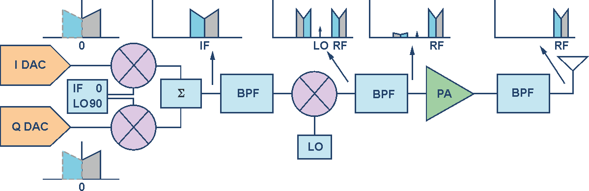
A classic radio transmitter implemented with a set of baseband high speed DACs is shown in Figure 1. The digital baseband data is sent through two synchronized high speed data converters, with in-phase data going through the I DAC and the quadrature data going through the Q DAC. The outputs of the DACs are sent to a quadrature modulator. Based on the type of modulator, its output can be a low intermediate frequency, such as 200 MHz to 400 MHz, a higher IF frequency such as 500 MHz to 1 GHz, or even an RF frequency in the 1 GHz to 5 GHz range. The diagram shows a subsequent upconversion to an eventual final frequency. The resulting signal is filtered with a band-pass filter and then sent through a power amplifier and another band-pass filter that may be part of a duplexer, for example.
 |
||
| Figure 1. | Illustration of a classic super heterodyne transmitter using high speed data converters. | |
The instantaneous bandwidth that is typically transmitted with such an architecture is tens to a few hundred MHz, limited mainly by the converter, power amplifier, and filter bandwidths. This is not enough for some systems, such as new E-band microwave backhaul radios that require 500 MHz, 1 GHz, or even 2 GHz radio channels. If a multiband radio is considered, such as might be implemented in a wireless infrastructure base station, an equally wide spacing of 500 MHz or 700 MHz or even 1 GHz may be required to cover some band combinations. A conventional radio would address that by implementing two radios, one for each band. It may be more desirable to combine radios into one radio chain, whether it be for cost or size or some other factor. In this case, a new approach is needed.
Enabling Technology
The focus of technology development in high speed data converters has long been to push the rate of data conversion higher while maintaining a consistent performance figure of merit. The figure of merit includes such items as noise spectral density (NSD) and spurious-free dynamic range (SFDR). Intermodulation distortion (IMD) is also important, both with single-tone signals as well as modulated signals, such as those in popular wireless communications systems like GSM and 3G (WCDMA) and 4G (OFDM), and cable applications where 256 QAM is used.
Higher rates of data conversion bring several advantages to the radio designer. First, the signal’s image is pushed higher in frequency, making the design of the analog reconstruction filter simpler and more realizable. In addition, higher update rates create wider first Nyquist zones, which in turn enable the converter to directly synthesize higher output frequencies. When the directly synthesized signal is high enough, an entire stage of analog frequency translation, or upconversion, can be removed from the radio, simplifying frequency planning and reducing the power consumption and size of the radio. Higher update rates also increase the amount of bandwidth available to spread the quantization noise of the data converter, giving processing gain to the transmitter’s noise spectral density.
As CMOS process technology has advanced, the addition of signal processing to data converters has become commonplace. The added feature sets of NCOs and interpolators in DACs relieves the FPGA or ASIC from the burden and power consumption of implementing those features, and enables the DACs to operate on lower data transfer rates than otherwise would be required. The lower data rates reduces overall power consumption in the system, and in some cases makes it possible for the digital chip, on which the fabric speed may range up to 300 MHz to 400 MHz, to keep pace with the converter. Having NCOs on chip enable the first frequency translation in a radio to happen in the digital domain, and so it is common to find intermediate frequencies in the hundreds of MHz in today’s radios, enabled by NCOs and interpolators on data converters.
Signal Processing RF DAC
What has changed with RF data converters is the ultimate update rate at which the RF converter is able to operate, and the addition of signal processing also capable of handling those speeds. This powerful combination of feature set and speed can enable dramatic changes to radio architecture design and opens new possibilities of reconfigurable and software-defined radios.
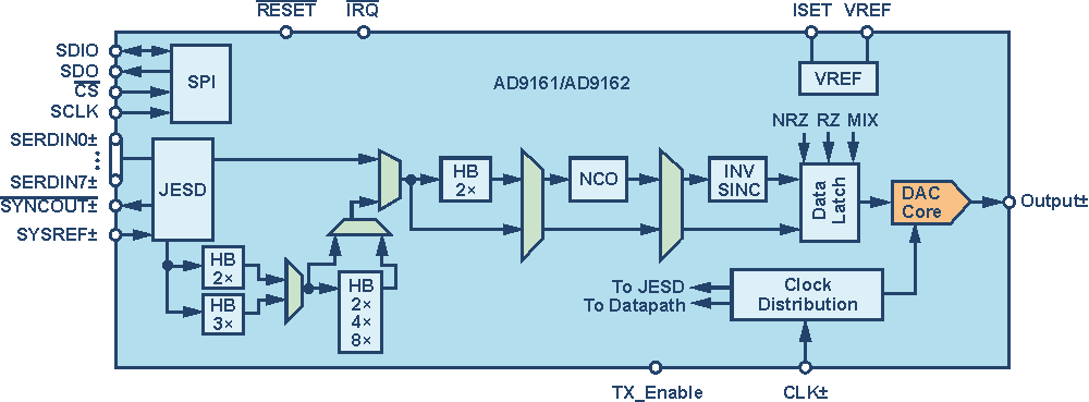
A good example of this is the AD9162 and AD9164 series of RF DACs. A block diagram of the AD9162 and AD9164 is shown in Figure 2. The AD9162 is a 16-bit, 6 GSPS RF DAC with several options of interpolation, from 1× bypass mode up to 24× interpolation. The interpolators operate on a classic 80% bandwidth or a wider 90% bandwidth for more instantaneous signal bandwidth at slightly higher power. The datapath also has a final half-band interpolator, FIR85, shown as the “HB 2×” block prior to the NCO in Figure 2, that effectively doubles the DAC update rate to up to 12 GSPS, moving images further away and easing filtering requirements. The optional FIR85 is followed by a 48-bit numerically controlled oscillator (NCO) that operates at either the 6 GSPS update rate or the 12 GSPS update rate when FIR85 is enabled. Following the NCO is an x/sinx compensation filter that corrects for the sinx/x roll-off of the DAC by pre-emphasizing the input to the DAC core.
 |
||
| Figure 2. | Block diagram of the AD9162 and AD9164 family of RF DACs. | |
The DAC core is designed with Analog Devices’ patented Quad Switch architecture, delivering superior spurious-free dynamic range (SFDR) and noise spectral density (NSD), resulting in the industry’s best dynamic range, while also providing the familiar DAC decoder options the Quad Switch enables: non-return-to-zero (NRZ) mode, return-to-zero (RZ) mode, and Mix-Mode™. The FIR85 adds a new feature to the DAC decoder called 2xNRZ mode, which will be described in more detail later.
The AD9164 has the base features of the AD9162, and it adds a direct digital synthesis (DDS) function in the form of a fast frequency hopping (FFH) NCO engine. The FFH NCO has several unique features that make it quite attractive for markets such as high speed test instrumentation, local oscillator replacement, secure radio communications, and radar exciters. The FFH NCO engine is implemented with thirty-two 32-bit NCOs, each with its own phase accumulator, and a selection block that enables the fast frequency hopping.
The AD9162 has two derivative products that are directed to specific markets. The AD9161 is an 11-bit, 6 GSPS RF DAC that has a minimum 2× interpolation. The SFDR and NSD of the AD9161 are suitable for cable head end and remote PHY applications and meet DOCSIS 3.0 specifications. The reduced signal bandwidth and dynamic range remove requirements for an export license for the AD9161. The AD9163 is a 16-bit, 6 GSPS RF DAC that has minimum 6× interpolation and retains the full dynamic range of the main product AD9162. The full dynamic range of the device and its wide 1 GHz instantaneous bandwidth plus full range NCO make the device suitable for single-band or dual-band wireless infrastructure base stations and also point-to-point microwave systems in the traditional bands, while also having the benefit of not requiring an export license. Table 1 summarizes the product family and key features.
| Table 1. | Summary of AD9162 and AD9164 Family of 6 GSPS RF DAC Features and Target Markets |
||||||||||||||||||||||||||||||
|
|||||||||||||||||||||||||||||||
Digital Datapath Highlights
Data is passed to the AD9162 and AD9164 by an 8-lane, 12.5 GBPS JESD204B interface. This high speed serial interface simplifies board layout complexity by reducing the number of wires needed to connect the digital baseband device to the DAC. A detailed guide to operation of the interface is given in the data sheet, and a comprehensive guide to the JESD204B interface is given on the Analog Devices website.
The first interpolator in the AD9162 and AD9164 datapath is either a 2× half-band or a 3× third-band filter. Either of these filters has a selectable 80% or 90% signal bandwidth. Both filters have 85 dB or greater of stop-band rejection. The 90% filters operate at higher power due to their sharper cutoff characteristic and therefore higher number of taps. The remaining 2× half-band filters all operate at 90% bandwidth to accommodate either of the first interpolators. The FIR85 also operates at 90% bandwidth. Because all of the subsequent filters are further down the line of interpolation, they can operate on the 90% bandwidth with an almost unnoticed increase in power.
The FIR85, which implements 2xNRZ mode when enabled, is implemented differently from the other interpolator filters. It takes advantage of the Quad Switch architecture of the DAC and uses the rising and falling edges of the DAC clock to sample data. This sampling method samples new data at each edge of the clock, and so it acts to double the sample rate of the DAC to up to 12 GSPS. This pushes the signal’s image to 2×fDAC – fOUT from fDAC – fOUT, making it easier to filter the images with more realizable analog filters. This method of sampling and interpolating makes the DAC output more sensitive to clock balance, but there are adjustments to the DAC clock input that can be used to tune for better performance. These adjustments are made by programming registers through the serial peripheral interface (SPI). Details are given in the data sheet.
The 48-bit NCO is a full quadrature NCO that enables image-free frequency shifting of the input data signal or direct digital synthesis of a single tone. The NCO has two selectable modes of operation, either phase continuous or phase discontinuous frequency switching. In phase continuous switching, the frequency tuning word (FTW) is updated but the phase accumulator is not reset, resulting in a continuous phase change in frequency. In phase discontinuous mode, the phase accumulator is reset when the FTW is updated. The serial peripheral interface (SPI) is guaranteed to 100 MHz to enable fast updating of the FTW.
The AD9164 adds an important feature to the NCO – the fast frequency hopping NCO (FFH NCO). The FFH NCO is implemented with an additional thirty-one 32-bit NCOs, each with their own phase accumulator. Each NCO has its own FTW, so that a total of 32 NCO FTWs can be programmed in the device. An FTW select register is provided so that a single SPI register byte write can accomplish a hop to a new frequency with accuracy to 32 bits. With the 100 MHz SPI, this means a new FTW can be chosen in 240 ns, with the single byte write.
The FFH NCO has an additional phase coherent frequency hopping mode that makes it attractive for instrumentation and military applications. Phase coherent frequency hopping is important for test applications and also radar applications that need to track the phase of an exciter signal for use later. Phase coherent frequency hopping enables changing from one frequency to another and back to the original one again, without losing track of the original frequency’s phase accumulation. Stated another way, it enables changing from one frequency to another and back again, and appearing as though the frequency was never changed.
Applications and Measured Performance
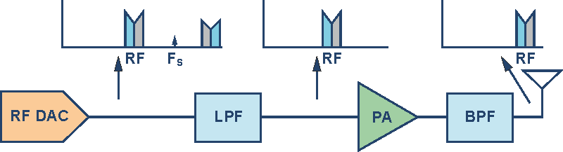
The signal processing features and high sample rate of the AD9162 and AD9164 enable a simplification of the radio architecture in Figure 1. The updated drawing is shown in Figure 3. Because the RF data converter can directly synthesize signals at the desired output frequency, there is no longer a need for a quadrature modulator or an upconverting mixer. The signal is created in the digital processor and simply played out of the RF data converter. The amount of hardware needed to implement the transmitter is thus greatly reduced. In addition, the radio is simpler to implement, with no need to calibrate the LO and DAC inputs to a quadrature modulator to suppress LO leakage and unwanted image, because the modulator is implemented digitally inside the RF data converter.
 |
||
| Figure 3. | Radio transmitter architecture implemented with an RF data converter. | |
 |
||
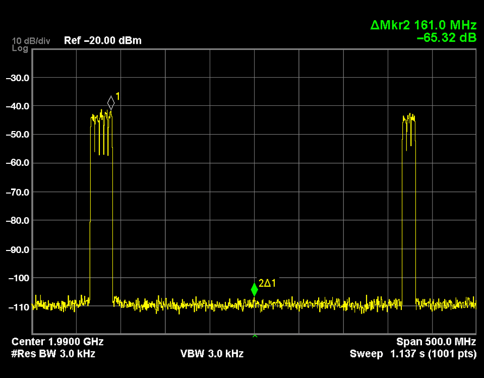
| Figure 4. | Dual-band WCDMA signal at 1.8 GHz and 2.1 GHz bands. | |
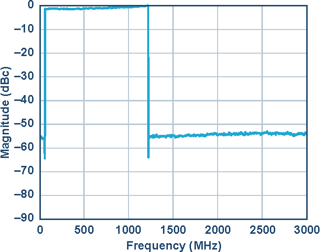
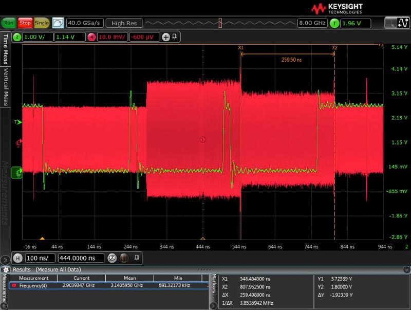
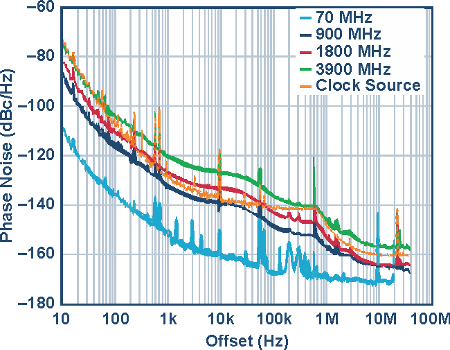
This type of architecture, with only an analog low-pass filter to filter the data converter’s image, opens up possibilities for reconfigurable or software-defined radios. The same digital part, RF data converter, and reconstruction low-pass filter could be used, with only a power amplifier and band-pass filter change, to implement a number of different radios. Figure 4 shows an example of a wireless base station dual-band transmitter output of five 5 MHz WCDMA carriers at 1800 MHz and three 5 MHz WCDMA carriers at 2100 MHz. Figure 5 shows an example of a compliant cable head-end transmitter output of 194 6 MHz wide 256 QAM carriers in the 50 MHz to 1.2 GHz spectrum of DOCSIS 3.1. Figure 6 shows an example of a fast frequency hopping dwell time of 260 ns, with 240 ns of register programming (single byte write) and 20 ns of hop time. Figure 7 shows the excellent phase noise performance of the AD9164, with better than –125 dBc/Hz at 10 kHz offset when running from a 4 GHz ovenized crystal oscillator and synthesizing a 3.9 GHz sine wave.
 |
||
| Figure 5. | 194 6 MHz 256 QAM signals in the DOCSIS 3.1 frequency band (50 MHz to 1.2 GHz). |
|
 |
||
| Figure 6. | Fast frequency hopping performance of the AD9164 – 260 ns dwell time per hop. |
|
 |
||
| Figure 7. | Aggregate phase noise performance of the AD9164. DAC clock signal source: 4 GHz ovenized crystal oscillator up to 600 kHz offset, then signal generator above 600 kHz offset. |
|
Conclusion
RF data converters can simplify radio architecture designs and reduce their size by eliminating many components from the radio signal chain. The AD9162 and AD9164 combine an exciting set of features and superior RF performance into an RF data converter that is able to address a wide range of radio transmitter applications, demonstrating that the reality of a truly software-defined radio is closer than ever.
