Alan Walsh, Analog Devices
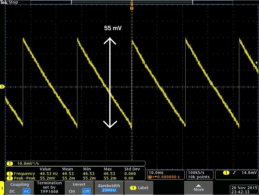
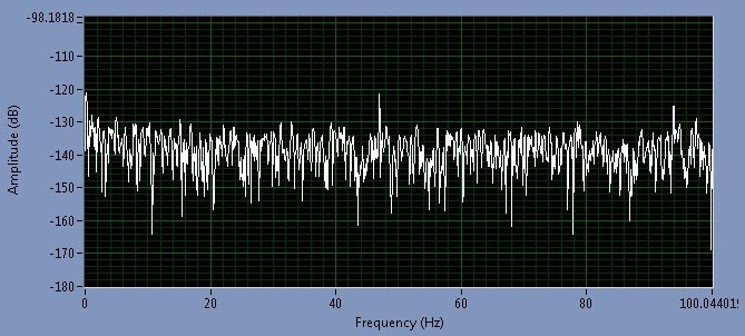
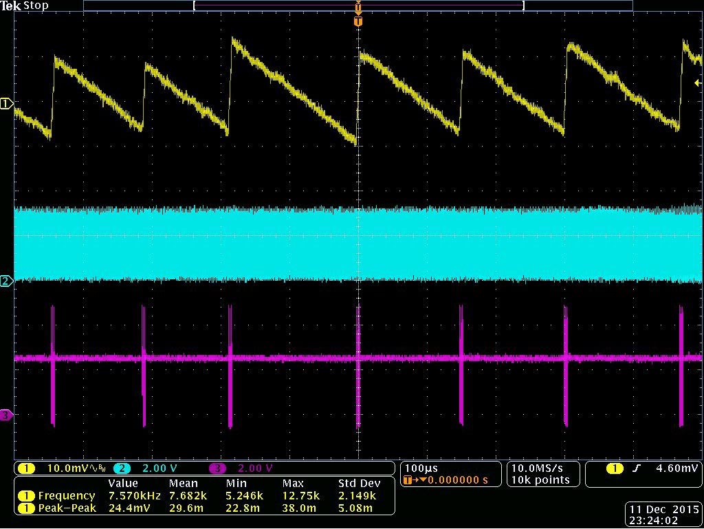
If the ADC throughput is reduced to 10 kSPS then the current consumption of the ADC scales linearly down to 15 μA (factor of ~100) and correspondingly, the switching frequency ripple of the ADP5300 scales to 46.5 Hz (factor of ~100) with an amplitude of 55 mV peak-to-peak, as seen in Figure 5. The ripple shows up in the ADC FFT output at 46 Hz again with an amplitude of –120 dB (5 μV peak-to-peak) because the PSRR is similar at this frequency. There is evidence of a second harmonic at 93 Hz that is –125 dB down.
 |
||
 |
||
| Figure 5. | ADP5300 hysteretic switching ripple (ac-coupled) when supplying the AD7980 and ripple tone in ADC FFT output at 10 kSPS throughput. |
|
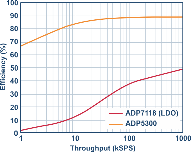
Figure 6 shows how the efficiency of the ADP5300 stacks up vs. that of an LDO across ADC throughput rate when regulating a 2.5 V output from a 5 V rail. As you would expect, the switcher is far more efficient at delivering power than the LDO, 90% vs. 50% (for a 5 V input) at 1 MSPS and holds up much better at lower ADC throughputs/lower current consumption, staying above 80% until 5 kSPS.
 |
||
| Figure 6. | Efficiency vs. ADC throughput for ADP5300 and LDO. | |
At an ADC throughput of 1 MSPS using an LDO, the current consumed from a 5 V rail is 1.5 mA or 7.5 mW. Using the ADP5300, the current consumed from a 5 V rail is 828 μA or 4.1 mW. This is a 3.4 mW or 45% reduction in the power drawn by the ADC power supply.
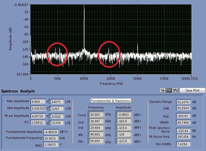
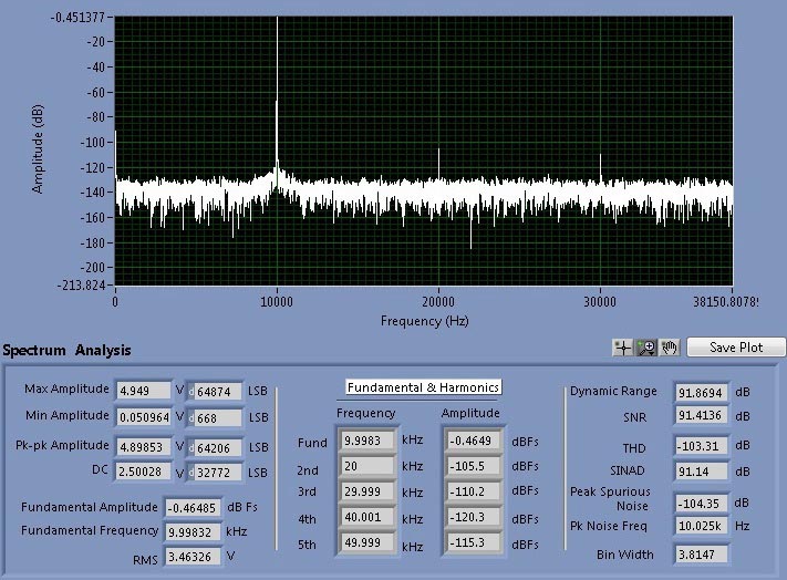
The performance of the AD7980 at 1 MSPS using the ADP5300 as the VDD supply is shown in Figure 7 with a 10 kHz almost full-scale input signal (–0.5 dB). The ADC still meets data sheet specifications in terms of SNR (91.5 dB) and THD (–103 dB). However, the ADP5300 switching ripple at 4.5 kHz gets modulated on top of the input signal and appears as spurs at 10 kHz – 4.5 kHz (5.5 kHz) and 10 kHz + 4.5 kHz (14.5 kHz). These spurs are still at a very low level (–116 dBFS) and much less than the THD introduced by the second harmonic of the fundamental signal (–103.8 dBFS at 20 kHz). These artifacts are a small fraction of an LSB at the 16-bit level, so in many applications it will be perfectly acceptable for the power savings of the ADP5300 regulator.
 |
||
| Figure 7. | Performance of AD7980 using ADP5300 as VDD supply. Side bands due to switching ripple modulation can be seen around the fundamental signal (10 kHz ±4.5 kHz). |
|
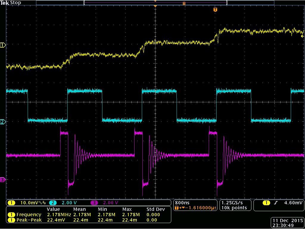
There is a STOP switching feature on the ADP5300 switcher that can completely eliminate these switching ripple artifacts from showing up in the ADC FFT output. The STOP pin on the ADP5300 prevents the SW pin from switching when STOP is held high. This can be used to prevent any switching from occurring during the noise sensitive conversion process of the ADC. In order to achieve this the CNV signal and STOP signal are tied together (see Figure 3) and the CNV signal from the processor is timed to remain high during the conversion time of the ADC. In the case of the AD7980 this is 710 ns max and conversion is initiated on the CNV rising edge. The results are shown in Figure 8. The ripple frequency is more variable in this case, as there are only specific times when the SW node can turn on and regulate. Also note that the SW turn-on time from the STOP signal going low can be hundreds of ns. In Figure 8, the SW pin turns on ~850 ns after the falling edge of STOP. This means we cannot use the STOP feature at 1 MSPS ADC throughput as the VDD supply will fall out of regulation and collapse, as there is insufficient time for the SW pin to go high and regulate. Instead, the STOP function will work for throughputs of 500 kSPS and lower.
 |
||
 |
||
| Figure 8. | ADP5300 switching ripple (yellow) with STOP function at 500 kSPS throughput, CNV/STOP signal (blue), and SW pin of ADP5300 (pink). |
|
As can be seen in Figure 9, the switching ripple spur is completely eliminated from the ADC noise floor with the use of the STOP signal. When an input signal of 10 kHz is applied there is no modulation or artifacts around the fundamental, apart from the normal harmonics. However, there is an efficiency hit for using the STOP feature due to ringing on the SW pin when the SW pin is disabled (STOP high). The efficiency of the ADP5300 with an ADC throughput of 500 kHz drops to ~75%. This is still considerably higher than the efficiency possible with an LDO (<50%) and gives the option of a power/performance trade-off that can be made in the application under the control of the processor/microcontroller if a separate control line is used for the STOP feature.
 |
||
 |
||
| Figure 9. | Performance of AD7980 using ADP5300 as VDD supply with STOP feature timed to conversion period. |
|
The cost and PCB area of a switcher solution like the ADP5300 is comparable to that of an LDO. The main addition to the BOM is a chip inductor, a 2.2 μH inductor can be as small as 0603 size, with the input and output caps already being required for an LDO solution. This makes it an attractive alternative to using an LDO in power sensitive applications without significantly impacting precision performance.
High efficiency, ultralow power switching regulators like the ADP5300 result in 45% power savings over LDOs when powering precision ADCs like the AD7980 from a 5 V rail. This has many benefits in IoT applications, extending battery life in wireless sensor nodes or wearable fitness devices, power sensitive isolated industrial systems, and 4 mA to 20 mA loop-powered systems.
