Single chip integrates an ARM processor, software defined modem and RF transceiver; supports the growing number of digital protocols
The MC13260 System-on-Chip (SoC) Two-Way Radio is a single-chip integrated microcontroller, software-defined modem, and RF transceiver intended for use in the two-way radio market. The MC13260 SoC Two-Way Radio incorporates a 32-bit ARM9 microcontroller, a highly optimized software-defined vector modem processor, a high-performance sub-1GHz transceiver achieving higher frequencies with external components, and mixed-signal analog circuits for voice and peripheral support. The overall design and programmability of MC13260 enables rapid time to market for multi-mode products, such as dual-mode analog/digital radios.
The high level of integration provides support for a comprehensive radio platform in a single package without the requirement of an additional external processor. This results in a small board area and a cost-effective solution. The MC13260 SoC Two-Way Radio provides a wide range of wireless communication protocol options, supporting both analog and digital modulation schemes.
The ARM926EJ-S provides flexibility and sufficient computational performance to execute a variety of speech and audio CODECs for use in digital voice communication, alerts, or music playback. The software-defined modem is a highly optimized vector digital signal processor enabling the implementation of analog and digital protocols, as well as enabling simple upgrade capabilities through software as standards evolve.
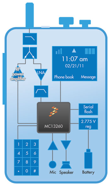
A complete two-way radio can be built using the MC13260 System-on-Chip Two-Way Radio as shown in Figure below.
The MC13260 SoC Two-Way Radio provides the following device level features:
- ARM9 Platform
- ARM926EJ-S core supporting clock speed up to 150 MHz.
- EmbeddedICE logic.
- Five-stage pipeline for ARM/Thumb.
- Five-stage pipeline for Java.
- External co-processor interface.
- MMU, instruction and data caches.
- Caches are virtually indexed and virtually addressed.
- Supports ARM, Thumb, and Java.
- Supports a JTAG port compliant to the ARM Debug Architecture.
- Modem Engine
- Programmable architecture; flexibility to implement a variety of functionality using the same hardware.
- Supports both real and complex modes of operation.
- 52-bit fixed length VLIW instruction format.
- Employs SIMD Architecture.
- Nine-stage pipeline for instruction and data processing.
- Uses 16-bit floating-point number representation thus offering a wide dynamic range.
- Single clock cycle execution typical for modem macro-instruction.
- DMEM which supports a 128-bit data read/write in each cycle.
- Register bank of eight registers, each 128-bits wide.
- The register bank supports 6 reads and up to 3 writes per cycle.
- Two Arithmetic Units (AU), each unit is:
- Capable of producing one complex multiply-and-add result, or
- Four real multiply-and-add results in one clock cycle.
- Produces one Decimation in Frequency (DIF) FFT or Decimation in Time (DIT) FFT butterfly per cycle.
- Supports four levels of nested hardware loops.
- Supports 8-deep Return Address Stack for subroutine calls.
- Special Arithmetic Unit (SAU) to perform several common special arithmetic operations for example, 1/x, 1/sqrt(x),1/(1+exp(|x|)), log(x) and so on, by using look-up tables.
- Comparator unit capable of minima/maxima search.
- Conversion from fixed-point representation to floating-point representation and vice versa on-the-fly.
- Supports conditional and unconditional program jumps and subroutine calls.
- General Purpose Unit (GPU) capable of some logical and arithmetic operations, for example, logical AND, OR, NOT, EXOR and so on, besides arithmetic/logical shift operations.
- Transceiver
- Contains receive, transmit, and frequency generation subsystems.
- Contains high fidelity converters for sub-MHz signals.
- Capable of an RF frequency range of 60 MHz–960 MHz with a frequency resolution of 1 Hz or less.
- High performance synthesizer achieves 75 dB adjacent channel selectivity.
- Provides configurable RF data channel bandwidth from 6.25 kHz–600 kHz.
- Contains one general purpose A/D and three general purpose D/A converters.
- Supports an extended operating frequency range up to 3 GHz with external circuitry.
- Supports linear transmit using an external modulator.
- Voice CODEC
- Digital Peripherals
- Advanced Security Module (ASM)
- Clock Monitor (CLKMON)
- Clock Control Module (CCM)
- Provides a mechanism to switch from one clock source to another without any glitch generation
- Two clock sources comprise a high speed clock, CKIH, and low speed clock, CKIL.
- Implements integral clock dividers
- Manages various low-power modes defined for the SoC.
- Configurable Serial Peripheral Interface (CSPI)
- Deep Sleep Module (DSM)
- Enhanced Periodic Interrupt Timer (EPIT)
- 32-bit down counter with clock source selection.
- 12-bit prescaler for division of input clock frequency.
- Counter value can be programmed on the fly.
- Can be programmed to be active in low-power and debug modes.
- Interrupt generation when counter reaches the Compare value.
- General Purpose Input/Output (GPIO)
- General purpose input/output logic:
- Ability to drive a specific data to the pad using DR register.
- Ability to control the direction of the pad using the GDIR register.
- The core is able to sample the status of the corresponding pads by reading the PSR register.
- GPIO interrupts support:
- Up to 32 interrupts.
- Ability to identify interrupt edges.
- Generate three one-bit interrupt lines to the SoC interrupt controller.
- General purpose input/output logic:
- General Purpose Analog-to-Digital Converter (GPADC)
- General Purpose Timer (GPT)
- One 32-bit up-counter with clock source selection, including external clock.
- Two input capture channels with programmable trigger edge.
- Three output compare channels with programmable output mode.
- Supports forced compare feature.
- Can be programmed to be active in low-power and debug modes.
- Interrupt generation at capture, compare, rollover events.
- Restart or free-run modes for counter operation.
- High-Performance Direct Memory Access (HDMA)
- Inter-Integrated Circuit (I2C)
- IC Identification Module (IIM)
- Provides interface to the fusebanks, allowing fuses to be read or programmed.
- Fuses may be programmed by software, directly by JTAG, or indirectly by JTAG via a processor.
- Ability to override fuse values in software (does not affect the fuse element); override capability can be permanently disabled.
- Ability to write-protect e-Fuses.
- Ability to scan-protect (read and program).
- KeyPad Port (KPP)
- Supports a key pad matrix of up to 5 rows × 4 columns.
- Port pins can be used as general purpose I/O.
- Open drain design.
- Glitch suppression circuit design.
- Multiple keys detection.
- Long key press detection.
- Standby key press detection.
- Synchronizer chain clear.
- Double-edge interrupts to enable multiple keys detect or N-key rollover.
- Pulse-Width Modulator (PWM)
- Two selectable input clock sources.
- 16-bit resolution.
- Two stage input clock divider (2, 4, 8, 16-divider and 7-bit prescaler).
- Programmable through four user-accessible 32-bit registers.
- 4 × 16 bit FIFO with associated status and interrupts.
- Software Reset function available to reset the entire PWM subsystem.
- Random Number Generator (RNGB)
- Real Time Clock (RTC)
- System Reset Control (SRC)
- Controls the Reset of the SoC.
- Controls the operation of CLKMONs and the power management functions.
- Synchronous Serial Interface (SSI)
- Smart LCD Controller (SLCDC)
- Transfers data from the display memory buffer to the external display device.
- Direct Memory Access (DMA) transfers the data transparently with minimal software intervention.
- Bus utilization of the DMA is controllable and deterministic.
- Reduce the CPU’s involvement in the transfer of data from memory to the display device.
- Transfers are optimized by using Direct Memory Access (DMA).
- After transfer is complete, a maskable interrupt is generated indicating the status.
- Supports Serial and parallel interfaces.
- Supports only writes to the display controller. Read operations from the display controller are not supported.
- Two 32 × 8-bit FIFOs.
- Control and status registers are accessible via the IP bus.
- Configurable to write image data to an external LCD controller via a 4-line serial, 3-line serial, an 8-bit parallel interface.
- Transfers data from the display memory buffer to the external display device.
- Timer Module (TMR)
- Four 16-bit counters/timers.
- Counts up/down.
- Counters are cascadable.
- Supports programmable modulo count.
- Maximum count rate equals peripheral clock/2 for external clocks.
- Maximum count rate equals peripheral clock for internal clocks.
- Count once or repeatedly.
- Counters are pre-loadable.
- Compare Registers are pre-loadable.
- Counters can share available input pins.
- Separate prescaler for each counter.
- Each counter has capture and compare capability.
- Timer Count Increment/Decrement Disable via DIS_L1T Input.
- Universal Asynchronous Receiver/Transmitter (UART1, UART2)
- USB Full Speed Device Controller (USB-FS)
- USB 2.0 compliant Full Speed device controller.
- Eight bidirectional End Points.
- Support control, isochronous, bulk and interrupt End Point types.
- DMA or FIFO data stream interface.
- Low-power suspend mode.
- USB Transceiver
- Complies with Universal Serial Bus Specification, Revision 2.0.
- Runs at low (1.5 Mbps) and full (12 Mbps) speeds.
- Converts USB differential voltages to a digital logic signal and vice versa.
- Supports a 3.5 meter maximum cable length connected to the USB data bus.
- Watchdog Timer (WDOG)
- RF/Analog Interfacing Peripherals
- General Purpose Analog-to-Digital Converter Interface (GPADC-IF)
- IP bus interface for ARM.
- Interrupt generation.
- Generation of control signals to the analog GPADC circuit.
- Schedules data conversions on the multiplexed A/D inputs.
- GPADC can be triggered by software or Transceiver Sequence Manager.
- RF Data Interface (RFDI)
- Provides bus interface for Rx and Tx data.
- Contains a multistage decimation filter to convert slow data rate to fast date rate.
- Contains a multi-stage interpolation filter to convert fast date rate to slow date rate.
- Rx FIFO to provide temporary data storage on receiving data path.
- SYNTH FIFO to provide temporary data storage on frequency synthesis data path.
- Operations to be controlled by TSM.
- Supports TxIQ mode allowing the RFDI block to provide the I and Q data to the high speed DACs.
- Transceiver Sequence Manager (TSM)
- Up to 32 sequence events for either:
- Separated Rx/Tx warm-up/warm-down events, or
- Combined warm-up / warm-down events.
- Triggered by pre-selected timer from TMR module (Timer Module).
- Programmable selection between Receive or Transmit Sequence.
- Supports autonomous execution of an already-started sequence without host core intervention.
- Start sequences either synchronized with TMR timer, or initiated by setting a start signal.
- Directly or indirectly (delayed from a signal being set) initiated warmdown sequence.
- Three maskable interrupt signals are generated to the ARM9 core at the end of sequences.
- Allow software overriding of its outputs.
- Up to 32 sequence events for either:
- Transmit Power Ramp Control (TPRC1, TPRC2, TPRC3)
- TSM controls ramp direction and ramp trigger.
- MCU programs the ramp profile into LUT for each PA stage. Loaded before ramp trigger.
- MCU programs target power for each PA stage. Loaded before ramp trigger.
- MCU programs duration and ramp step which determines the number of L1 clocks in between samples.
- Each TPRC controls one of the three DACs
- Enables DAC selection to determine whether one, two, or three DACs are enabled during ramping.
- MCU controls ramp bypass to apply static target power value to input of DAC.
- Supports a bypass mode to allow direct streaming of I and Q data from RFDI to the GPDACs.
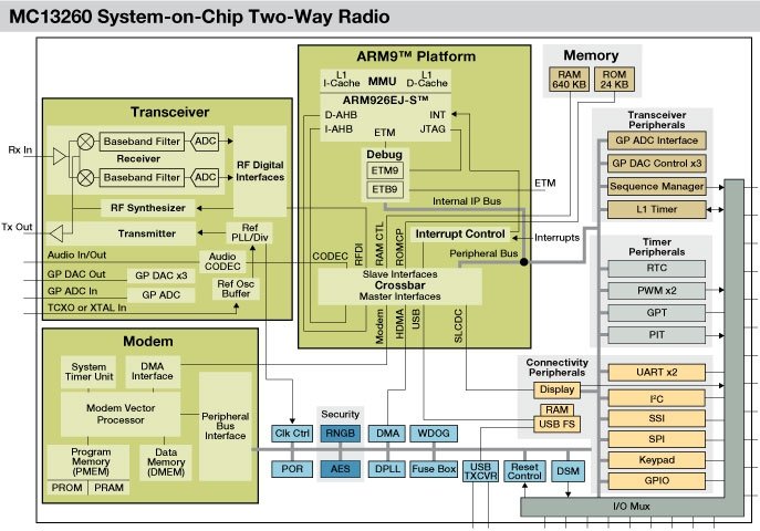
MC13260 SoC block Diagram