RF Monolithics, AN0901
Introduction
 |
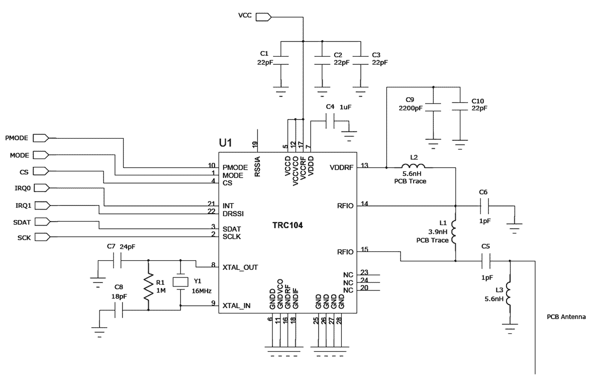
This application note presents a PCB reference design for RFM’s TRC104 2.4 GHz transceiver IC. The reference design, including a PCB antenna, easily fits on one square inch of circuit board. Two RF inductors are implemented as circuit board traces, avoiding the cost of discrete inductors. The reference design schematic is shown in Figure 1 below. |
 Click to enlarge |
|
| Figure 1. | TRC104 Reference Design Schematic |
Bill of Materials
The TRC104 Reference Design BOM is presented below:
|
U1
|
RFM TRC104 2.4 GHz Transceiver IC
|
|
Y1
|
Crystal, 16.00000 MHz, RFM XTL1021 or equivalent
|
|
R1
|
1 M ±5%, 0.1 W, 0402
|
|
C1, C2, C3, C10
|
22 pF ±5% NPO, 0402
|
|
C4
|
1 μF ±10% COG, 0402
|
|
C5, C6
|
1 pF ±5% NPO, 0402
|
|
C7
|
24 pF ±5% NPO, 0402
|
|
C8
|
18 pF ±5% NPO, 0402
|
|
C9
|
2200 pF ±5% NPO, 0402
|
|
L3
|
5.6 nH ± 10% 0402
|
Circuit Board Layers
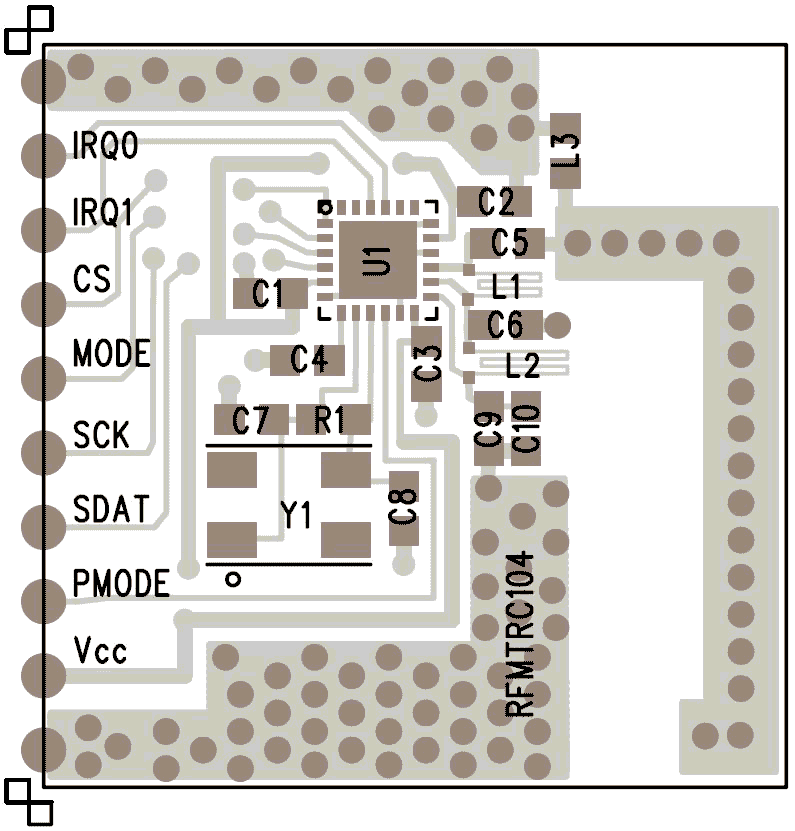
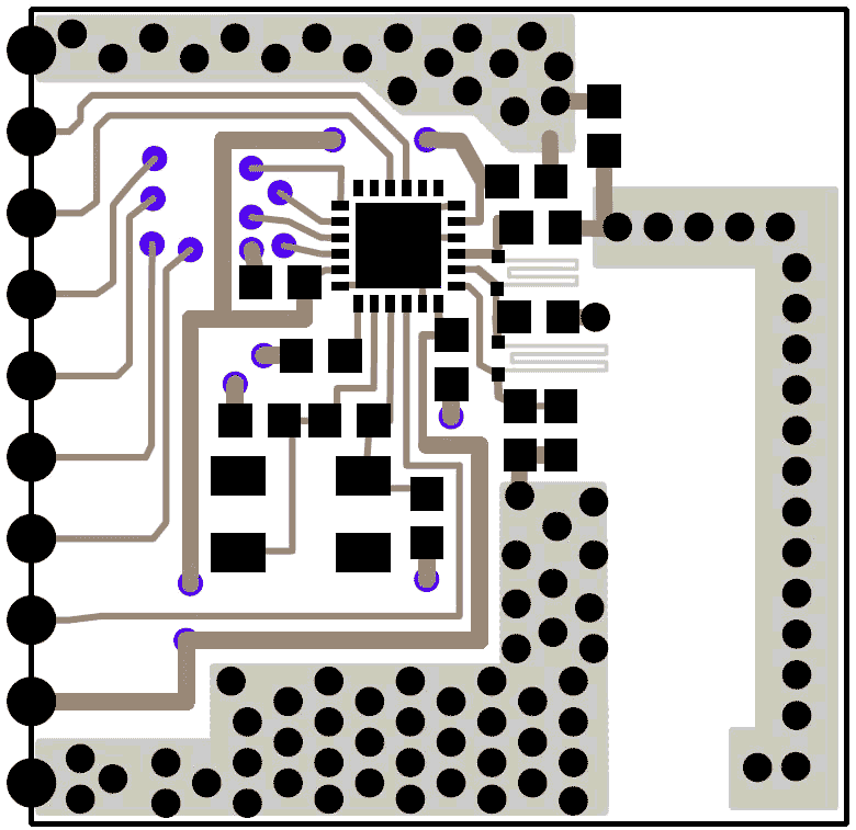
Figure 2 shows the TRC104 reference design top assembly. Power supply and digital I/O signals are organized on the left, the printed antenna is on the right. A wide variety of microcontrollers can be used to control the TRC104. Note RF inductors L1 and L2 are implemented as circuit board traces. PADs PCB design files and Gerber files of the reference design layout are available here.
 Click to enlarge |
 Click to enlarge |
||
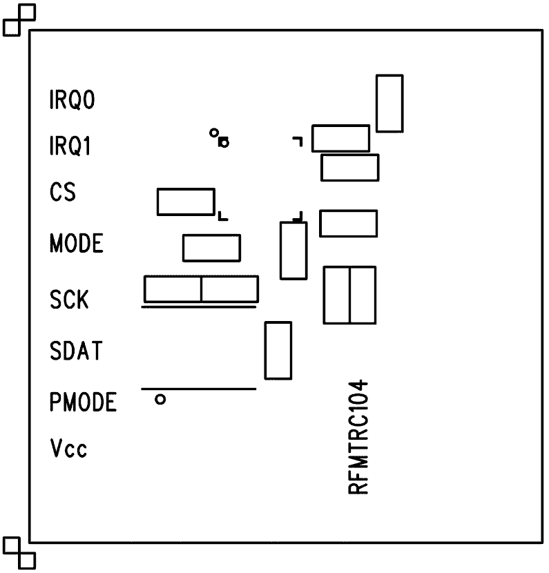
| Figure 2. | Top Assembly | Figure 3. | Top Silkscreen |
The top silkscreen is shown in Figure 3 above.
 Click to enlarge |
 Click to enlarge |
||
| Figure 4. | Top Solder Mask | Figure 5. | Top Etch |
The top solder mask is shown in Figure 4.
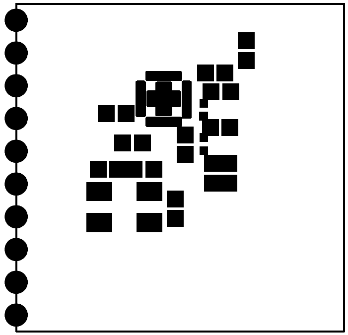
The top etch pattern is shown in Figure 5. Using ±5% NPO RF capacitors where specified in the bill of materials is important to reference design performance.
 Click to enlarge |
|
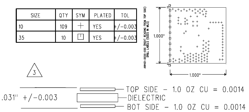
| Figure 6. | Drill & Layer Data |
The drill and layer data is provided in Figure 6. The reference design is implemented on a two-sided 0.031 inch board with 1 oz copper traces.
 Click to enlarge |
 Click to enlarge |
||
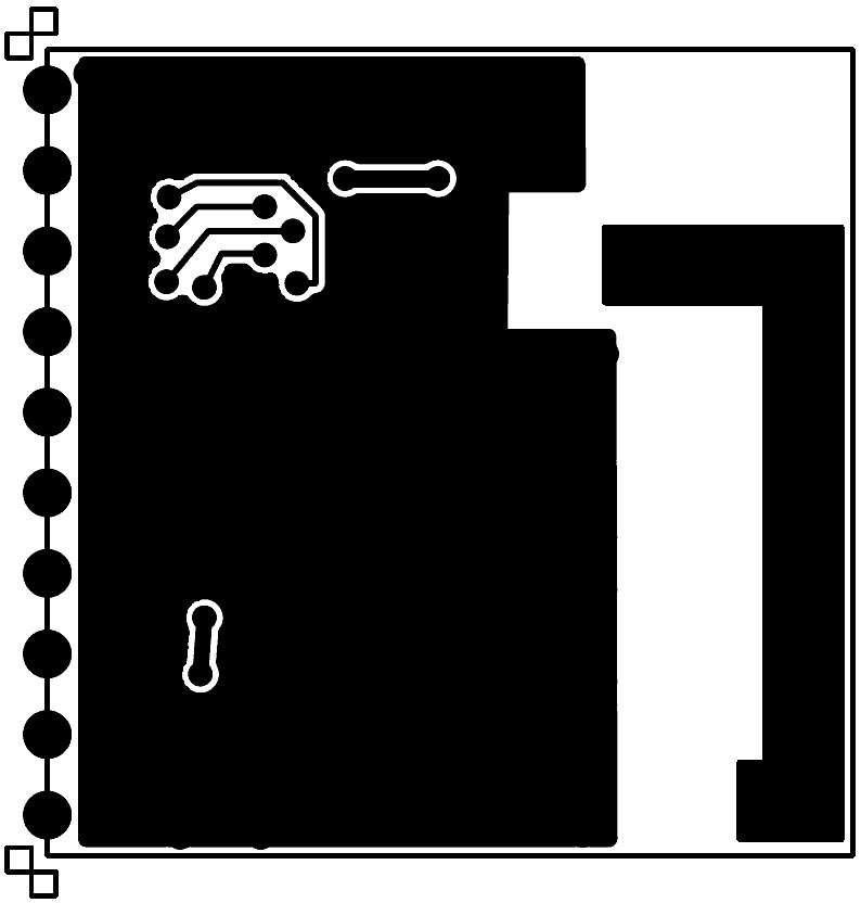
| Figure 7. | Bottom Etch | Figure 8. | Bottom Solder Mask |
Figure 7 shows the reference design bottom etch pattern.
Figure 8 shows the TRC104 reference design bottom solder mask.
 |
|
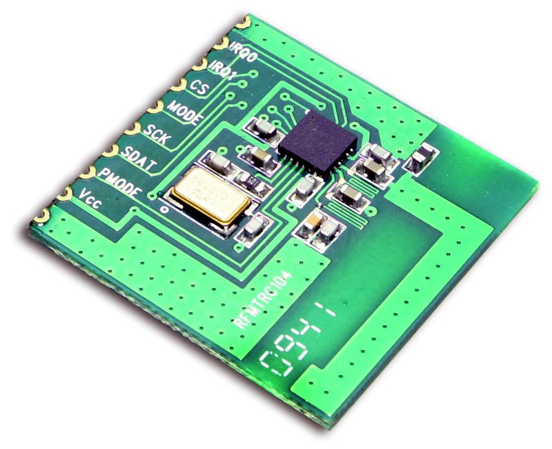
| Figure 9. | Assembled Reference Design PCB |
Figure 9 shows the assembled TRC104 reference design PCB.
Minimizing Sleep Mode Current
Several TRC104 digital I/O lines must held logic low to achieve minimum sleep mode current, as discussed in Section 4.1 of the TRC104 data sheet:
- SDAT
- SCLK
- INT
- RSSID
These lines can be held low by the host microcontroller during sleep mode, or the host microcontroller pins can be tri-stated and 100K pull-down resistors can be used. Note that the 100K pull-down resistors are not included on the TRC104 reference design.
Reference Design Testing
The TRC104 reference design has been tested in a variety of office environments and typically achieves an operating range of 50 feet (15 meters) when transmitting data at 1 Mb/s.
