The added output has its own voltage regulation
Designers use step-up-converter ICs in battery-powered portable equipment. These chips usually provide one output with a fixed or an adjustable voltage. Some chips contain an LBI/LBO (low-battery-in/low-battery-out) function. The chip manufacturer intends for these pins to be used for monitoring a low-battery condition and to warn gadget owners when a battery goes flat. You can instead use this function to provide an extra voltage output.
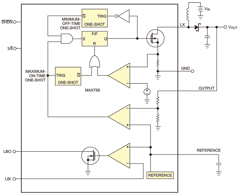
The Maxim MAX756 boost converter provides a fixed output of 3.3 or 5V at 300 and 200 mA, respectively (Figure 1). The input voltage can range from 0.7 to 5.5V. For low-battery detection, the part has on-chip circuitry comprising a comparator, a reference, and an open-drain MOSFET. When the voltage at the LBI input is lower than its threshold level of 1.25V, the MOSFET at the LBO output sinks current to ground.
 |
|
| Figure 1. | You can use the battery-monitoring circuit in this fixed-output boost converter to make a secondary output voltage (courtesy Maxim). |
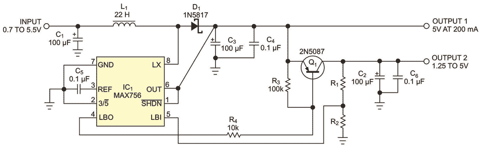
You can use these components to make a second output with a regulated voltage (Figure 2). R1 and R2 determine the secondary output voltage according to the following equation: Output 2 =VREF(R1+R2)/R2, where VREF is the reference voltage, which is 1.25V for this chip.
 |
|
| Figure 2. | You can use the LBI and LBO pins of this boost-converter IC to operate a low-dropout secondary output. |
You can set Output 2 from 1.25 to 5V as long as it is less than Output 1. Because Output 2 is derived from Output 1, the total output current for both outputs should not exceed 200 and 300 mA for Output 1 and Output 2 voltages of 5 and 3.3V, respectively.
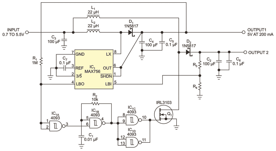
You can also use the LBI/LBO function to make a second boost converter (Figure 3). The CD4093 quad Schmitt-triggered NAND gates, inductor L2, R2 through R4, Q1, D1, C1, and C2 compose this boost converter. Add C1 and R2 to IC1B to make a free-running oscillator that IC1A gates on. For the values of R2 and C1 in the figure, the oscillator frequency is approximately 17 kHz. R1 pulls up the open-drain LBO output.
 |
|
| Figure 3. | If you need a boosted secondary output, you can use the LBI and LBO pins to make another switching boost converter. |
When the voltage at the LBI pin is lower than 1.25V, the LBO pin is low, thus allowing operation of the IC1B oscillator. IC1C and IC1D drive power MOSFET transistor Q1. When Q1 is on, it pulls current from inductor L1. When Q1 is off, this energy charges capacitor C2 through flyback diode D1. You apply feedback with resistor divider R3 and R4 to determine the Output 2 voltage, according to the following equation: Output 2=1.25V×(R3+R4)/R4. IC1 gets power from Output 1.
 |
|
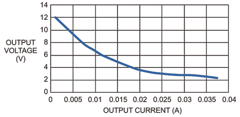
| Figure 4. | With only 1V input, the circuit cannot hold regulation, and the output voltage drops directly with output current. |
The voltage at Output 2 is a function of the output current and the input voltage (Figure 4). If you have adequate input voltage, the output graph shows a flat section where the IC’s regulation is effective (figures 5 and 6).
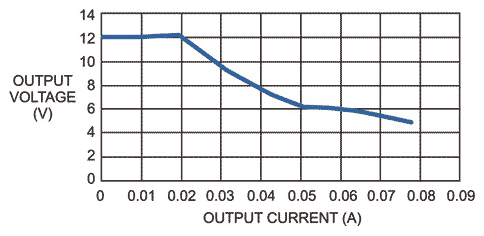 |
|
| Figure 5. | With a 2V input, the circuit maintains regulation to an output current as high as 20 mA. |
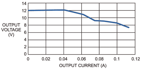 |
|
| Figure 6. | With a 3V input, the circuit holds regulation to an output current as high as 40 mA. |
