Raju Baddi, Tata Institute of Fundamental Research, Pune, India
EDN
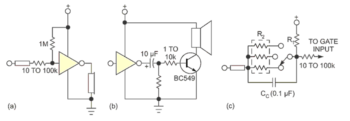
It is sometimes useful to listen to an audio signal at a test-circuit point. The 4069, with its high input impedance and sufficient output drive current of approximately 6.8 mA, can drive a small PCB-mountable speaker. That approach lets you build a simple audio probe (Figure 4). The resistor at the gate input of Figure 4a protects the gate if the unit under test has voltages higher than the gate supply voltage.
 |
|
| Figure 4. | A resistor at the gate input protects the gate if the unit under test has voltages higher than the gate supply voltage (a). A small resistor can be added in series with the speaker to control volume and prevent possible speaker or transistor damage (b). In an optional method of biasing the gate input for enhanced sensitivity, various R2 values are possible (c). |
Two methods of driving the acoustic transducer are shown, depending on the loudness requirements. Figure 4a shows a direct connection to a piezo transducer. For the louder sound of a speaker, a small resistor can be added in series with the speaker of Figure 4b to control volume and prevent possible speaker or transistor damage. Figure 4c shows an optional method of biasing the gate input for enhanced sensitivity.
The biasing voltage is given by the voltage divider network using this equation:
![]()
where
- VS is the supply voltage,
- ξ is the duty cycle (TH/(TH+TL)) of the input signal (assumed to be a rectangular wave),
- VH is the logic-high voltage, and VL is the logic-low voltage.
A suggested value for R1 is 1 MΩ; the user can choose R2 (suggested to be 1 MΩ) according to the equation for biasing voltage. Various R2 values are possible, as the switching arrangement in Figure 4c shows. Capacitor CC (suggested to be 0.1 μF) acts in series with the signal to be investigated and supplies the biasing voltage in series with the signal. The minimum strength of the signal is limited by the input threshold window of the gate and is different for different logic gates. For a rectangular signal changing between zero and the signal voltage, for example, the biasing voltage should be below the threshold window, and the value of the biasing voltage plus the signal voltage should be above the threshold window.
A stringent situation exists when those two values lie just at the edge of the window. So, for a rectangular or attenuated digital signal,
![]()
is the minimum required signal strength. In general, gates differ in ΔVT; some have wide widths (CD4069) and others narrow widths (CD4011). When an ac signal such as a sine wave is applied, however, the negative phase of the signal reduces the biasing voltage by its strength to VB−VSIG. It is thus sufficient that one phase produces a change equal to half of the window width. For ac signals, therefore, the minimum signal-strength criterion is VSIG=ΔVT/2.
Finally, for an inverting gate,
![]()
where
- VT2 is the input voltage at which the output of the gate has completely settled to logic zero,
- VT1 is the input voltage at which the output of the gate has completely settled to logic one.
R1 and R2 help in choosing the critical signal strength above the minimum that the threshold window of the gate has set. If R2 is approximately 1 MΩ, then the R2CC time constant is 0.1 sec, which corresponds to 10 Hz and seems to be adequate.
For plain digital signals, it is enough to omit R2 and CC; in other words, both R2 and CC equal zero. It should be noted that this coupler does not remedy the stagnant signal condition, preventing a constant drain current at the output. It is intended to provide a typical transistor amplifier kind of biasing for the audio probe gate. The stagnant signal condition is taken care of with a series 10-μF capacitor at the gate output of Figure 4b.
Readers interested in using the traditional ac coupling (with the left terminal of R2 connected to ground instead of the probe tip) RC circuit may use the following formula to calculate the expected V'B as a function of various parameters:
![]()
where all of the terms have the usual meaning.
 |
|
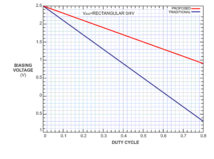
| Figure 5. | The input ac coupling of Figure 4c is less sensitive to duty cycle than is traditional series-capacitor ac coupling. |
Compare this equation with the previous equation. Whereas the biasing voltage in the equation for V'B depends on VH or VL through a single multiplicative factor of the duty cycle, in the equation for the biasing voltage it depends on another multiplicative factor,
thus reducing the dependence and producing a flatter profile with a duty cycle as shown in Figure 5 for a rectangular wave of
![]()
and a varying duty cycle.
You can assemble all of these gadgets in a small container, such as a glue-stick tube, and use the probe for a variety of tests (Reference 4). You can power the probe using two 3 V CR2032 lithium cells; the CMOS 4069 is a low-power device. Note, however, that 4069 devices from different manufacturers differ widely in their threshold voltages, so you should check that value before selecting a device to make the test gadgets, especially the first three.
 |
|
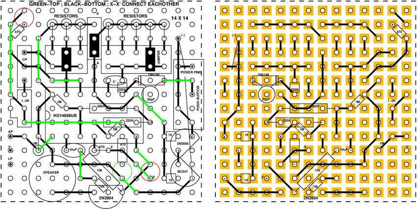
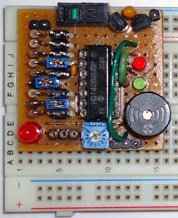
| Figure 6. | The circuit layout. |
The key to these test gadgets is the high input impedance of the CMOS gates. Other packages, such as the CD4011/4001, can also yield multiple gadgets because what matters is the use of the inverter gate.
 |
|
| Figure 7. | Circuit prototype photo. |
Editor’s note:
In all of the circuits discussed here, the probe ground should be connected directly to the unit-under-test ground. Although the Design Idea does not discuss it, some readers might want to add CD4011/4001 NAND/NOR logic to combine the continuity tester, astable oscillator, and audio probe to provide an audio tone for the continuity tester.
References
- Funk, RE, “Understanding Buffered and Unbuffered CD4xxxB Series Device Characteristics,” Texas Instruments, 2002.
- Baddi, Raju, “Test continuity with an LED,” EDN, Jan 6, 2011, pg 47.
- Baddi, Raju, “Detect live ac-mains lines,” EDN, Nov 4, 2010, pg 48.
- Baddi, Raju, “Probing system lets you test digital ICs,” EDN, June 21, 2012, pg 48.
