Application Note AN4391
November 2013
Delfo Fusillo, Filippo Scrimizzi
P-channel and N-channel MOSFETs show a different electrical performance. Due to lower hole mobility (three times smaller than electrons), the magnitude of specific on-resistance is greater in the P-channel structure. A larger die-size is needed to reach the same RDS(on) performance. However, an important advantage of P-channel devices is the simplicity and the driving circuitry optimization. In this document, new STripFET VI DeepGATE trench Pchannel technology is deeply analyzed, from a technological point of view and in some of most popular applications for P-channel FETs, such as: low power DC-DC conversions (buck, boost) and load switches.
P-channel MOSFETs don't play a relevant role in high-current applications, where a low RDS(on) is required to minimize the system conduction losses. In fact, with the same diesize, the P-channel device's RDS(on) is around 2.5/3 times higher than N-channel one, in other words, a bigger die-size for P-channel structures is needed to achieve the same onstate performance. This is a serious drawback in terms of overall system cost, efficiency and thermal management when the system works at a high switching frequency. If the die-size is bigger, device's intrinsic capacitances and switching losses are higher. However, there are several application segments where P-channel FETs can be used with a good performance ...
![]() Download Application Note AN4391 (1.7 Mb)
Download Application Note AN4391 (1.7 Mb)
Related datasheets:
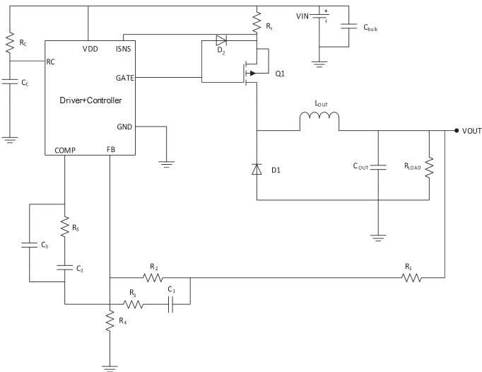
Non synchronous buck converter schematic
