Tyler Hutchison and Clarence Mayott, Linear Technology
Design Note 1031
Introduction
High speed ADCs use a sample and hold input structure comprising a fast CMOS switch and a sampling capacitor. When the CMOS switch closes, the sampling capacitor shares its stored charge with the preceding drive circuitry (charge kickback). As the sampling capacitor and its stored charge increase in size, more attention must be paid to the drive circuitry.
Pipeline ADCs typically have a few picofarads of sample capacitance. In contrast, the high performance 16-bit 20 Msps LTCR2270 high speed ADC uses a 17 pF sampling capacitor. The advantage of a relatively large sampling capacitor is a significant reduction of internal kT/C noise and therefore better signal-to-noise ratio (SNR). The disadvantage is that the part becomes more difficult to drive. Every time the CMOS switch closes, the sampling capacitor kicks back significantly more charge to the driver than would a smaller sampling capacitor.
The interface filter, between the driver and ADC, demands extra attention. An inappropriate filter deteriorates SNR and SFDR. This filter must limit noise, and also adequately settle charge kickback to protect the driver and the ADC from reflections. This design note shows how to design a suitable driver and 10 MHz interface filter for the LTC2270.
Driver Selection
The LTC2270 has a stellar 84.1 dB SNR (46 μVRMS input referred noise), in addition to 99 dB SFDR at baseband. To ensure that performance of the LTC2270 is optimum, the ADC driver must be tolerant to large charge kickbacks, drive a relatively heavy load and have low wideband noise.
Common mode termination on the ADC input, necessary to maintain the low distortion of the ADC, results in a significant load for the driver. Additionally, the driver must be extremely low noise. As a point of reference, a 3 nV/√Hz amplifier across a 10 MHz bandwidth would deteriorate the SNR by more than 1 dB. The LTC6409 is a good choice to meet these requirements. It provides drive and output swing to allow for enough common mode termination and an input referred voltage noise of 1.1 nV/√Hz.
Filter Design
High frequency pipeline ADCs digitize an enormous bandwidth of information. The LTC2270 exhibits a full power bandwidth of 200 MHz, enabling it to digitize 20 Nyquist zones and integrate wideband noise distortion, clocking frequencies and other radio frequency artifacts.
 |
|
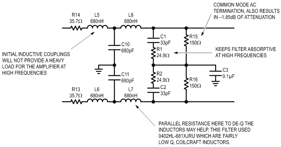
| Figure 1. | An Interface Filter of Approximately 10 MHz Used Between the LTC6409 and the LTC2270. |
The interface filter limits the broadband noise from the driver, but without careful design, the filter can also deteriorate the SFDR. To obtain optimum SFDR specifications for the driver and the ADC, start with these broad guidelines:
- Тhe ADC should see low impedance from its inputs. Since sampling is primarily a common mode effect, this termination should be common mode.
- The driver should see relatively high impedance, especially when driving the ADC to full-scale.
- Filters with absorptive (never open or short) characteristics behave better.
- A common mode termination capacitor mitigates the effect of charge kickback on the driver and the ADC. A filter that contains common mode termination and properly settles charge kickback will optimize SFDR.
 |
|
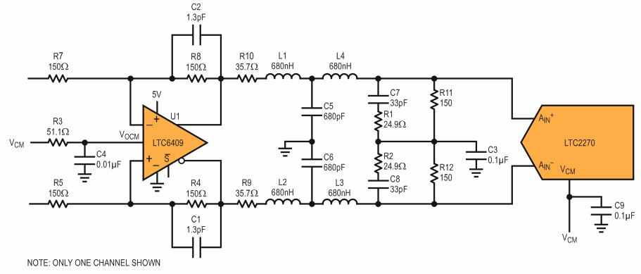
| Figure 2. | The Full ADC Interface Including the LTC6409 as a Buffer, a 10 MHz Lowpass Filter, and the LTC2270. |
There are other interface filter design guidelines, especially concerning layout, but these considerations provide some basic direction. The filter in Figure 1 illustrates these specifications and performs well in lab. Figure 2 shows the full interface.
Lab Testing
The proper filter and termination for a particular design must be experimentally verified, as there is no single rule or equation that covers all setups. Lab tests ensure that the filter can tolerate these circuit realities, such as board parasitics. Lab tests can also prove that resistive and reactive termination can have a significant impact on system distortion.
 |
|
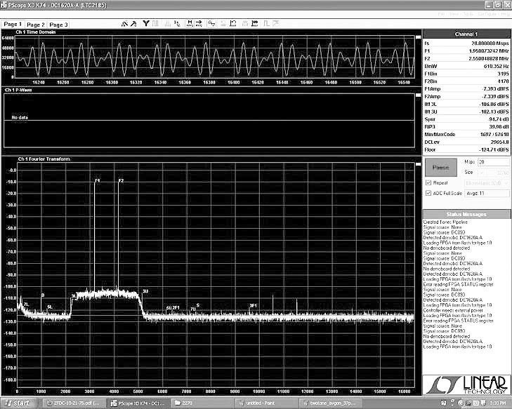
| Figure 3. | 2-Tone Spectrum of the LTC2270. The Heightened Noise Floor is Due to the Signal Generator. |
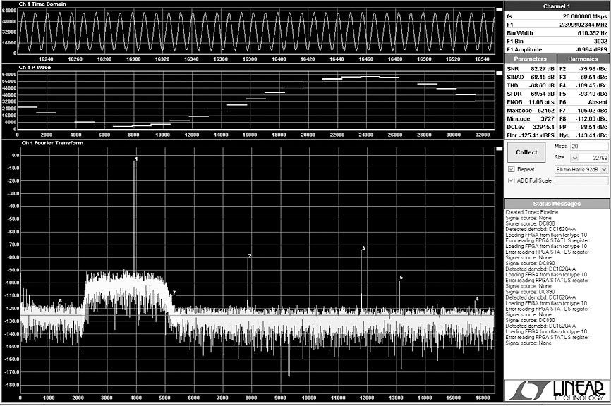
For instance, Figure 3 shows a 2-tone test performed using the interface in Figure 2. Additionally, Figure 4 shows the distortion deterioration between absorptive termination and no-output termination. The in-band SFDR is better than 100 dB and the SNR has only been deteriorated by 0.4 dB. Lab results may also display unexpected excess noise or distortion. In most cases, some amount of tweaking is necessary. For instance, reducing the bandwidth may increase SNR, but often at the expense of distortion.
 |
|
 |
|
| Figure 4. | Spectrum of the LTC2270 Sampling a 2.4MHz Sinusoid at 20Msps. (Top) SFDR Is Quite Poor When All Output Termination Has Been Removed from the Interface Filter. (Bottom) The Intended Filter Shows Near Data Sheet Specifications in Terms of SNR and Distortion. |
Here are a few practical rules to keep in mind for interface filter design:
- Keep the filter symmetric in value and layout
- Use only low distortion capacitors like COG/NPO, de-Q or use Low Q filter inductors
- Provide common-mode roll-off
Conclusion
Despite the LTC2270’s additional sample capacitance, a suitable driver and 10 MHz filter provide almost no deterioration to the LTC2270’s data sheet specifications. While the LTC6409 may work with the LTC2270 to digitize higher frequencies, the filter design may not be as straightforward as replacing inductors and capacitors with scaled values. In the end, use bench testing to produce empirical evidence to prove the adequacy of any ADC interface.
