Chapin Wong, Maxim Integrated
Application Note 5978
Certain applications require the use of a negative voltage reference, which is usually not readily available. A common way to generate a negative voltage has been to use an operational amplifier (op amp) to invert the output of a positive precision voltage reference. This approach typically requires a positive reference, the op amp, and two supply rails to generate the negative output.
Another approach to generate the negative supply rail uses a charge-pump inverter. This method requires a voltage reference, a charge pump, an op amp, and a positive supply rail. While these methods work, they each require several components and consume more space than is really ideal. Plus, the numerous components add cost, which is undesirable.
This article presents a simple way to generate the negative voltage reference from a single supply using an op amp with an integrated charge pump. This op amp-charge pump combination is found on the MAX9820, which is actually a stereo headphone amplifier IC with various features for its intended applications. However, it serves another purpose here as the basis for a circuit that generates a negative voltage reference while requiring the fewest components and power-supply rails and reducing the bill of materials (BOM) and required board space.
Circuit Description
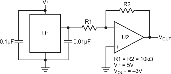
The circuit of Figure 1 uses a 3-V series reference (U1) and an op amp with internal charge pump (U2) to form a negative voltage reference. U1 provides an accurate 3-V output while consuming less than 5 µA. In this configuration, the output of U1 is connected to the feedback loop of U2. Negative feedback forces the output of the op amp to be –3 V. Low-output offset voltage on U2, combined with the precision accuracy of U1, enables a high-accuracy negative output voltage.
 |
|
| Figure 1. | This circuit generates a negative voltage reference. The U1 voltage reference (MAX6010A) drives the input of U2 op amp (MAX9820.) The output of U2 is a negative reference voltage. |
The supply voltage must be high enough to address any potential headroom issues with the voltage reference and the op amp. The voltage reference also requires a 3.2 V input voltage to generate a 3 V reference. The absolute maximum voltage on both U1 and U2 is 6 V; the highest recommended operating voltage on both parts is 5.5 V. The supply rail range for this circuit is a minimum of 3.2 V and a maximum of 5.5 V.
Decoupling capacitors are needed for the voltage reference. The recommended decoupling capacitance is 0.1 µF for the input and 0.01 µF for the output. U2 requires a 0.1 µF in parallel with a 10 µF.
 |
|
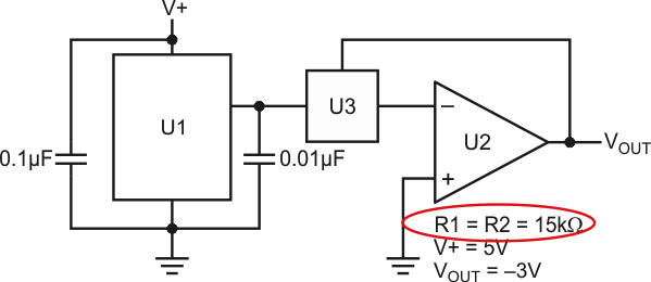
| Figure 2. | This diagram shows the Figure 1 circuit and the replacement of the two resistors with U3 (the MAX5491) precision matched resistor-divider. |
High-precision matched resistors should be used for R1 and R2 to ensure a stable output voltage across the entire temperature range of the two devices (–40 °C to +85 °C.)
There is a higher cost, but more accurate alternative to using two matched resistors in the feedback path: use a precision resistor-divider (Figure 2). As an example, the MAX5491 (U3) offers resistance matching of 0.035% (A grade), 0.05% (B grade), and 0.1% (C grade); it covers the entire operating temperature range of the voltage reference and op amp in the circuit. It is an ideal addition to this voltage regulator.
 |
|
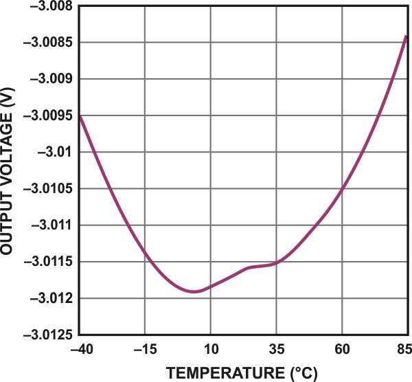
| Figure 3. | Output voltage versus temperature for the Figure 1 circuit under no load conditions. |
Figure 3 shows the output voltage versus temperature for the circuit in Figure 1. The maximum temperature deviation from –40 °C to +85 °C is 3 mV and within the output voltage maximum specifications of the U1 voltage reference as a standalone device.
 |
|
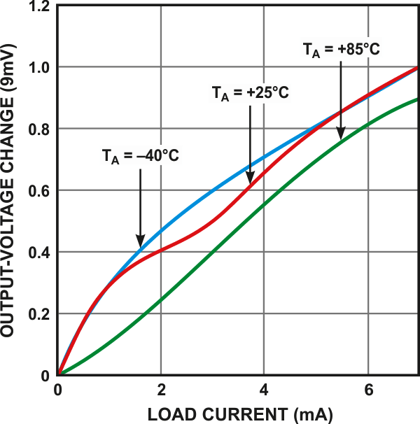
| Figure 4. | Output voltage versus load for the Figure 1 circuit. |
Figure 4 shows the output voltage versus load current at –40 °C, +25 °C, and +85 °C for the Figure 1 circuit. Testing was done with two 1% resistors in the feedback loop and a supply voltage of 5 V.
