Alfredo Saab
EDN
Analog applications, such as testing, calibration, and general system operation, often require a sine waveform of accurate amplitude and frequency, with low THD (total harmonic distortion). Some applications demand that the generator of such waveforms have the ability to accurately synchronize the output with an external timing signal. Simple sine-wave generators can offer various degrees of this performance, but maintaining low THD with constant amplitude is a problem, particularly if the output and the synchronization signal must remain locked through an extended range of frequencies.
 |
|
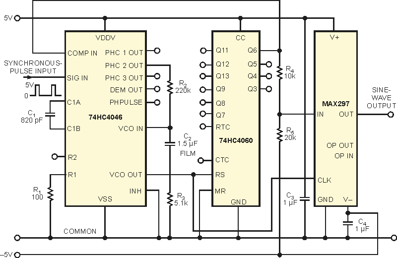
| Figure 1. | This three-IC sine-wave generator covers three frequency decades, provides low distortion, and allows you to synchronize it with an external signal. |
The circuit in Figure 1 can synchronize a sine-wave output through three decades of frequency – 20 Hz to 20 kHz – and maintain low THD and constant amplitude (Table 1). The synchronizer IC, an NXP Semiconductors 74HC4046, is a PLL (phase-locked loop) with a VCO (voltage-controlled oscillator) and a phase/frequency detector. It has three internal phase detectors, but this design uses the one with a frequency-capture range equal to that of the VCO-frequency range (the maximum frequency minus the minimum frequency).
| Table 1. | Amplitude versus frequency |
||||||||||||||||||||||
|
|||||||||||||||||||||||
The circuit’s general-purpose binary frequency divider, the 74HC4060, connects between the VCO output and the 74HC4046 feedback (phase/frequency-comparator) input and has a division ratio of 64. When the PLL is locked, therefore, the Q6 output of the 74HC4060 generates a square wave equal to 1/64th of the VCO-output frequency. The components that determine the 74HC4046 center frequency, C1 and R1, determine the VCO-frequency range from 20×64 to 20,000×64 from the minimum to the maximum level of the VCO’s input-voltage range.
A switched-capacitor lowpass filter, the Maxim MAX297, whose cut-off frequency by design equals 1/50th of the clock frequency you apply to it, has for signal input the same square wave it uses for the PLL feedback, and its clock input attaches to the VCO output. Because the clock and signal inputs always have a frequency ratio of 64, the input signal always falls within the filter bandpass. No input harmonics fall within this bandpass because the ratio of the clock frequency to frequency is less than 50 for all of them. (For the lowest second harmonic, the ratio is 32.) The THD, up to the 32nd harmonic, is lower than 0.1%.
The fact that the filter’s input signal is a square wave with a 50% duty cycle helps in this application because a square wave contains only odd harmonics of the fundamental, and the lowest-frequency harmonic is the third, which is well within the filter’s deep-attenuation range.
You can frequency-modulate the synchronization signal, but that task entails a compromise between the synchronization-tracking speed (or maximum modulation frequency and depth) and the frequency-locking range, which the PLL’s lowpass filter components, R2, R3, and C2, set. Modulation speed is limited for the values the figure shows because those values are optimized for an extended-frequency locking range. You can download more information, including a full data sheet for the MAX297 (Reference 1).
Reference
- “MAX293/MAX294/MAX297 8th-Order, Lowpass, Elliptic, Switched-Capacitor Filters, Revision 2,” June 2008, Maxim.
