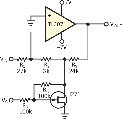
One problem with standard FET gain-control circuits is increased noise when you use the FET as a part of a resistive attenuator in series with an op amp. This configuration attenuates the signal before amplification; hence, it requires much higher gain bandwidth and better noise performance from the op amp. When you substitute the FET for the gain-setting resistor in a noninverting op-amp circuit, distortion limits the circuit configuration to applications in which the input voltage is less than a few hundred millivolts. The FET imposes this limitation, because the channel-depletion layer is a function of VDG and VGS. The improved circuit in Figure 1 uses the FET as part of the feedback loop.
 |
|
| Figure 1. | The drain-source resistance of the FET controls the gain of the op-amp stage. |
The voltage across the FET is limited in this application, and the noise performance is good. An added bonus is improved linearity performance. The transfer function for the improved circuit is as follows [1]:
When R2 + R3 = R1 and R4 = RDS (FET drain-source resistance), the transfer function reduces to
The minimum drain-source resistance for the FET on hand, J271, is 76 Ω at VGS = 0 V. The actual VDS at the inception of distortion varies with each FET, but keeping VDS lower than 200 mV usually prevents distortion. In the design in Figure 1, the FET drain-source voltage is limited to approximately 100 mV to prevent distortion. The divider action between R3 and RDS creates VDS from the output voltage, according to the following equation:
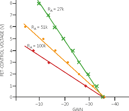
You can calculate R3 as 24.5 kΩ and select 24 kΩ. The parallel value of R2 and R3 determine the maximum circuit gain. Selecting R2 as 3 kΩ yields R1 equal to 27 kΩ and a maximum gain of –37. The measured gain at VC = VGS = 0 V is –36.1, which correlates well with the calculated value. RA and RB are feedback resistors that linearize the FET's VGS versus RDS transfer function. You can normally obtain adequate linearization with equal-value resistors, but you can also control the slope of the transfer function by setting the resistor ratio. The graph in Figure 2 shows that RA modifies the transfer function and linear control-voltage range (VGS). The p-channel FET, J271, requires a positive control voltage, but you can use a negative control voltage with an equivalent n-channel FET, such as the J210. The circuit is versatile and provides low distortion, wide range, good linearity, and low cost. The TLC071 op amp has low input-bias currents and has provisions for input offset-voltage correction.
 |
|
| Figure 2. | The ratio RA/RB in Figure 1 controls the slope of the gain-control transfer function. |
