Jim Williams
EDN
The VFC (voltage-to-frequency-converter) circuit in Figure 1 achieves a wider dynamic range and a higher full-scale output frequency – 100 MHz with 10% overrange to 110 MHz – by a factor of 10 over any commercially available converter. The circuit's 160-dB dynamic range spans eight decades for a 0 to 5 V input range and allows continuous operation down to 1 Hz. Additional specifications include 0.1% linearity, a 250-ppm/°C gain/temperature coefficient, a 1-Hz/°C zero-point shift, and a 0.1% frequency shift for a 10% power-supply- voltage variation. A single 5 V supply powers the circuit.
 |
||
| Figure 1. | Featuring a 160-dB dynamic range corresponding to a 1-Hz- to 100-MHz-frequency span, this voltage-to-frequency converter operates from a single 5 V power supply. |
|
Chopper-stabilized amplifier IC1, an LTC1150, controls a crude but wide-range oscillator core comprising bipolar transistors Q1 and Q2 and inverters IC2A and IC2B. In addition to delivering a logic-level output, the oscillator core clocks divide-by-four counter IC3, which in turn drives IC4, a 74HC4060 configured as a divide-by-16 counter.
After undergoing a total division by 64 in IC3 and IC4, the oscillator core's output drives a charge pump comprising IC5, an LTC6943, and its associated components. The averaged difference between the charge pump's output and the applied input voltage appears at the summing node and biases IC1, thereby closing the control loop around the wide-range oscillator core. The circuit's extraordinary dynamic range and high speed derive from the oscillator core's characteristics, the divider/charge-pump-based feedback loop, and IC1's low dc input errors. Both IC1 and IC5 help stabilize the circuit's operating point by contributing to overall linearity and stability. In addition, IC1's low offset drift ensures the circuit's 50-nV/Hz gain-versus-frequency characteristic slope and permits operation as low as 1 Hz at 25°C.
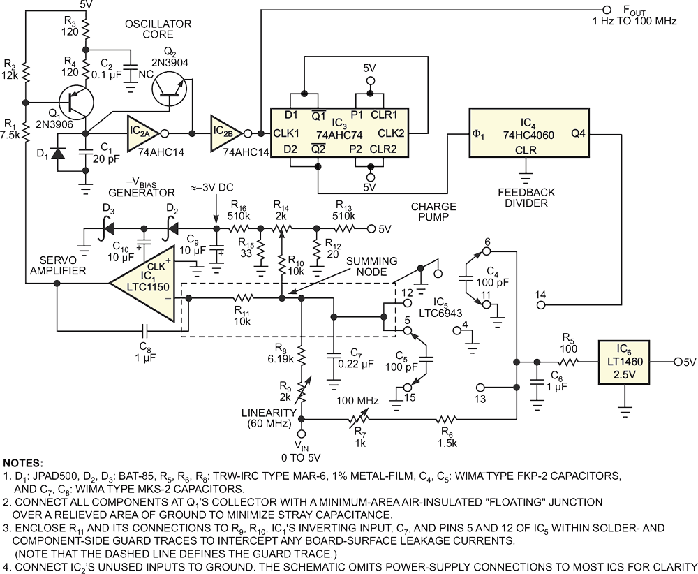
Applying a positive input voltage causes IC1's output to go negative and alter Q1's bias. In turn, Q1's collector current produces a voltage ramp on C1 (upper trace in Figure 2). The ramp's amplitude increases until Schmitt trigger inverter IC2A's output (lower trace in Figure 2) goes low, discharging C1 through Q2 (connected as a low-leakage diode). Discharging C1 resets IC2A's output to its high state, and the ramp-and-reset action continues.
 |
||
| Figure 2. | On a 700-MHz real-time oscilloscope, the oscillator-core waveforms at a 40-MHz operating frequency show the ramp-and-reset waveform at Q1’s collector (upper trace) and Q2’s emitter (lower trace). |
|
The leakage current of diode D1, a Linear Systems JPAD500, dominates all other parasitic currents in the oscillator core, but its 500-pA maximum leakage ensures operation as low as 1 Hz. The two sections of charge pump IC5 operate out of phase and transfer charge at each clock transition. Components critical to the charge pump's stability include a 2.5 V LT1460 voltage reference, IC6; two Wima FKP-2 polypropylene film/foils; 100-pF capacitors, C4 and C5; and the low charge-injection characteristics of IC5's internal switches.
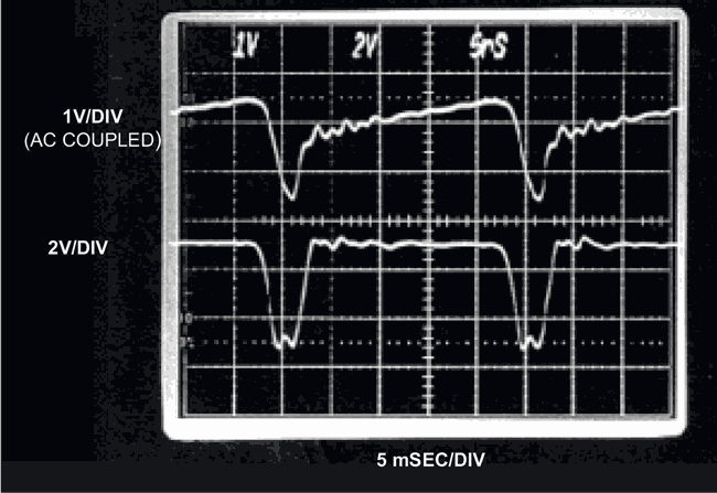
The 0.22-µF capacitor, C7, averages the difference signal between the input-derived current and the charge pump's output and applies the smoothed dc signal to amplifier IC1, which in turn controls the bias applied to Q1 and thus the circuit's operating point. As noted, the circuit's closed-loop-servo action reduces the oscillator's drift and enhances its high linearity. A 1-µF Wima MKS-2 metallized-film-construction capacitor, C8, compensates the servo loop's frequency response and ensures stability. Figure 3 illustrates the loop's well-behaved response (lower trace) to an input-voltage step (upper trace).
 |
||
| Figure 3. | In response to an input-voltage step (upper trace), the voltage at the circuit’s summing junction shows a 30-msec settling time. |
|
For the circuit to achieve its design goals, certain special techniques and considerations apply. Diode D1's leakage current dominates all other parasitic leakage currents at IC2A's input, and thus Q1 must always supply sufficient source current to sustain oscillation and ensure operation as low as 1 Hz.
The circuit's 100-MHz full-scale upper frequency limit forces stringent restrictions on the oscillator core's cycle time, and only 10 nsec is available for a complete ramp-and-reset sequence. The reset interval imposes an ultimate speed limit on the circuit, but the upper trace in Figure 2 shows a 6-nsec reset interval that falls comfortably within the 10-nsec limit. A path from the circuit's input to the charge pump's output allows for correction of small nonlinearities due to residual charge injection. This input-derived correction is effective because the charge injection's effects vary directly with the oscillation frequency, which the input voltage determines.
Although you can use the component values given in Figure 1 to assemble prototypes and small production quantities of the circuit, you need to consider component selection for optimum manufacturability and high-volume production. Table 1 lists certain components' target values and estimated selection yields. The notes in Figure 1 list the key components that the design uses.
| Table 1. | Selection criteria for components. | |||||||||||||||||||||
|
||||||||||||||||||||||
To calibrate the circuit, apply 5 V to the input and adjust the 100-MHz trimmer, R7 for a 100-MHz output. Next, connect the input to ground and adjust trimmer R14 for a 1-Hz output. Allow for an extended settling interval because, at this frequency, the charge-pump update occurs once every 32 sec. Note that R14's adjustment range accommodates either a positive or a negative offset voltage because IC1's clock output generates a negative bias voltage for R14. Next, apply 3 V to the input and adjust R9 for a 60-MHz output. A certain amount of interaction occurs among the adjustments, so repeat the process until you arrive at optimum values for the three calibration frequencies.
