Bill Reeve
Electronic Design
By adding only a few components, you can turn a temperature- and beta-compensated current sink into a common-emitter (CE) amplifier that maintains a stable biased operating point. This architecture is useful for building stable and device-tolerant BJT Class A amplifiers.
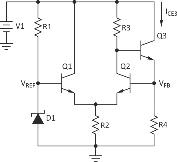
The circuit in Figure 1 sinks a constant current (ICE3) through Q3’s collector and emitter. This design is balanced so changes in Q3’s base-emitter voltage (VBE) don’t affect the current sink’s performance. Feedback around Q3 eliminates the circuit’s sensitivity to temperature-induced and component-to-component variations in Q3’s forward gain (beta).
 |
||
| Figure 1. | This temperature-compensated current-sink circuit is insensitive to the value of Q3's low-frequency current gain (beta). |
|
The circuit establishes a temperature- insensitive reference voltage (VREF) at the base of Q1 by using a Zener diode (D1) for which R1 sets the operating current. A 6.2-V Zener diode is ideal as it operates at a balance between true Zener behavior and avalanche breakdown. Alternatively, if you have less voltage headroom available, you could use a shunt bandgap reference such as the LM385 or even a simple resistive voltage divider if V1 is from a regulated supply.
Transistor Q1 operates as an emitter follower and sets its emitter voltage to be one base-emitter voltage drop (VBE) below VREF. As a result, it creates a stable reference voltage at the emitter of Q2. Transistor Q2 acts to throttle Q3’s base – and thus Q3’s collector-emitter current ICE3 – to keep the feedback voltage at the top of R4 (VFB) approximately equal to VREF.
If ICE3 rises, the IR drop across R4 increases Q2’s base voltage. This rise in base voltage increases Q2’s collector current through R3, dropping Q3’s base voltage, thus reducing ICE3. Similarly, if ICE3 drops, Q2’s base voltage decreases and reduces Q2’s collector current. Such current reduction lowers the IR drop across R3, raising Q3’s base voltage and increasing ICE3. This operation is independent of Q3’s low-frequency current gain (beta).
 |
||
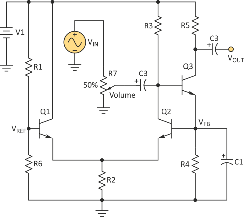
| Figure 2. | Adding a load resistance (R5), bias-voltage bypass capacitor (C1), and I/O coupling capacitors (C2, C3) turns the temperature- and beta-stable current sink into a simplified common-emitter (CE) amplifier. |
|
Because it has a stable collector-emitter bias current, Q3 can act as a voltage amplifier by adding a few components (Fig. 2). The first addition is a bypass capacitor (C1) across R4 to provide an ac current path while maintaining the dc bias current through R4. Adding ac coupling caps (C2 and C3) to carry the input and output voltages, a load resistor (R5) on Q3’s collector, and a volume-control potentiometer (R7) turns the circuit into a temperature- and beta-stable audio-frequency voltage amplifier. Note: this example uses R6 as part of a voltage divider rather than the Zener diode to set VREF.
 |
||
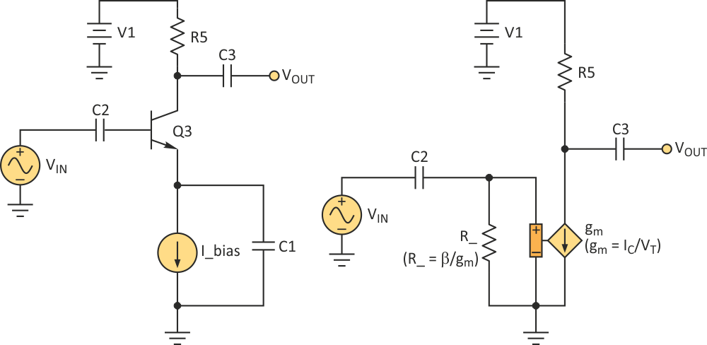
| Figure 3. | The amplifier's simplified schematic (a) allows derivation of the circuits small-signal model (b) for analysis. |
|
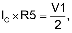
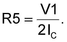
A simplified schematic of this common-emitter amplifier (Fig. 3a) lets us derive a small-signal model (Fig. 3b) for analysis. In this schematic, I_bias is Q3’s collector current (IC). To maximize the output voltage swing, we would ideally choose the load resistance R5 so Q3’s collector voltage is midway between the supply voltage (V1) and ground. Therefore:
or
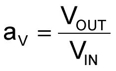
Note that the amplifier’s output voltage (VOUT) is given by:
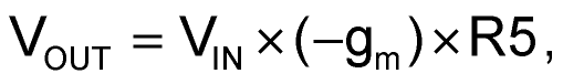
or
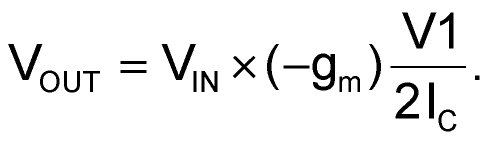
Because
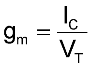
(where VT equals approximately 26 mV), the small signal voltage gain
is approximately:
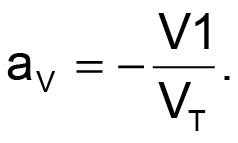
An audio-frequency voltage amplifier using the component values given in the Table 1 would have a maximum gain of approximately 45 dB.
| Table 1. | Audio frequency amplifier component values |
||||||||||||||||||||
|
|||||||||||||||||||||
