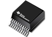
Datasheet Texas Instruments LMZ12010
| Manufacturer | Texas Instruments |
| Series | LMZ12010 |

10A SIMPLE SWITCHERВ® Power Module with 20V Maximum Input Voltage
Datasheets
LMZ12010 10-A SIMPLE SWITCHERВ® Power Module With 20-V Maximum Input Voltage datasheet
PDF, 1.4 Mb, Revision: H, File published: Sep 1, 2015
Extract from the document
Prices
Status
| LMZ12010TZ/NOPB | LMZ12010TZE/NOPB | |
|---|---|---|
| Lifecycle Status | Active (Recommended for new designs) | Active (Recommended for new designs) |
| Manufacture's Sample Availability | Yes | Yes |
Packaging
| LMZ12010TZ/NOPB | LMZ12010TZE/NOPB | |
|---|---|---|
| N | 1 | 2 |
| Pin | 11 | 11 |
| Package Type | NDY | NDY |
| Industry STD Term | TO-PMOD | TO-PMOD |
| JEDEC Code | S-MSFM-P | S-MSFM-P |
| Package QTY | 32 | 250 |
| Carrier | TUBE | SMALL T&R |
| Device Marking | LMZ12010 | LMZ12010 |
| Width (mm) | 15 | 15 |
| Length (mm) | 15 | 15 |
| Thickness (mm) | 5.9 | 5.9 |
| Pitch (mm) | 1.27 | 1.27 |
| Max Height (mm) | 6.13 | 6.13 |
| Mechanical Data | Download | Download |
Parametrics
| Parameters / Models | LMZ12010TZ/NOPB | LMZ12010TZE/NOPB |
|---|---|---|
| Iout(Max), A | 10 | 10 |
| Iq(Typ), mA | 1 | 1 |
| Operating Temperature Range, C | -40 to 85 | -40 to 85 |
| Package Size: mm2:W x L, PKG | See datasheet (PFM) | See datasheet (PFM) |
| Package Type | Leaded | Leaded |
| Regulated Outputs | 1 | 1 |
| Soft Start | Adjustable | Adjustable |
| Special Features | EMI Tested,Enable,Tracking | EMI Tested,Enable,Tracking |
| Switching Frequency(Max), kHz | 404 | 404 |
| Switching Frequency(Min), kHz | 314 | 314 |
| Switching Frequency(Typ), kHz | 359 | 359 |
| Vin(Max), V | 20 | 20 |
| Vin(Min), V | 6 | 6 |
| Vout(Max), V | 6 | 6 |
| Vout(Min), V | 0.8 | 0.8 |
Eco Plan
| LMZ12010TZ/NOPB | LMZ12010TZE/NOPB | |
|---|---|---|
| RoHS | Not Compliant | Not Compliant |
Application Notes
- Understanding and Applying Current-Mode Control TheoryPDF, 409 Kb, File published: Aug 19, 2007
- AN-643 EMI/RFI Board Design (Rev. B)PDF, 742 Kb, Revision: B, File published: May 3, 2004
Application Note 643 EMI/RFI Board Design - Input and Output Capacitor SelectionPDF, 219 Kb, File published: Sep 19, 2005
- AN-2145 Power Considerations for SDI Products (Rev. B)PDF, 63 Kb, Revision: B, File published: Apr 26, 2013
This application report discusses the issues and trade-offs that VCC ripple has on the performance of SDI components. - AN-2155 Layout Tips for EMI Reduction in DC/ DC Converters (Rev. A)PDF, 3.6 Mb, Revision: A, File published: Apr 23, 2013
This application note will explore how the layout of your DC/DC power supply can significantly affect theamount of EMI that it produces. It will discuss several variations of a layout analyze the results andprovide answers to some common EMI questions such whether or not to use a shielded inductor. - Design Summary LMZ1xxx and LMZ2xxx Power Module Family (Rev. B)PDF, 996 Kb, Revision: B, File published: Jan 20, 2016
- AN-2026 Effect of PCB Design on Thermal Performance of SIMPLE SWITCHER Modules (Rev. A)PDF, 455 Kb, Revision: A, File published: Apr 23, 2013
This application report focuses on the low current modules that come in a 7 lead, 10.16 x 4.57 x 9.81 mmpackage. - AN-1889 How to Measure the Loop Transfer Function of Power Supplies (Rev. A)PDF, 2.7 Mb, Revision: A, File published: Apr 23, 2013
This application report shows how to measure the critical points of a bode plot with only an audiogenerator (or simple signal generator) and an oscilloscope. The method is explained in an easy to followstep-by-step manner so that a power supply designer can start performing these measurements in a shortamount of time. - Semiconductor and IC Package Thermal Metrics (Rev. C)PDF, 201 Kb, Revision: C, File published: Apr 19, 2016
- AN-2020 Thermal Design By Insight, Not Hindsight (Rev. C)PDF, 568 Kb, Revision: C, File published: Apr 23, 2013
This application report provides an in-depth discussion of thermal design. - AN-2078 PCB Layout for Texas Instruments SIMPLE SWITCHER Power Modules (Rev. A)PDF, 1.1 Mb, Revision: A, File published: Apr 23, 2013
This application report discusses the best PCB layout methods, practices and techniques to maximize themodule’s performance. - AN-2052 Texas Instruments SIMPLE SWITCHER Power Modules and EMI (Rev. C)PDF, 99 Kb, Revision: C, File published: Apr 23, 2013
While the principles discussed in this application report apply more broadly to power design, we will focuson DC to DC convertor design given its broad application. It affects virtually every hardware engineer whoat some point has to design a power convertor. In this application report we will consider two commontrade-offs related to low EMI design; thermal performance and EMI and also solut - AN-2146 Power Design for SDI and Other Noise-Sensitive Devices (Rev. A)PDF, 1.4 Mb, Revision: A, File published: Apr 26, 2013
This application report discusses various solutions for meeting the power requirements of serial digital interface (SDI) video components. - AN-2027 Inverting Application for the LMZ14203 SIMPLE SWITCHER Power Module (Rev. A)PDF, 244 Kb, Revision: A, File published: May 6, 2013
This application report illustrates how to apply the LMZ14203 integrated buck module into the buck-boost configuration such that a positive input voltage can be used to create a regulated negative output voltage. - AN-1149 Layout Guidelines for Switching Power Supplies (Rev. C)PDF, 82 Kb, Revision: C, File published: Apr 23, 2013
When designing a high frequency switching regulated power supply layout is very important. Using agood layout can solve many problems associated with these types of supplies. The problems due to a badlayout are often seen at high current levels and are usually more obvious at large input to output voltagedifferentials. Some of the main problems are loss of regulation at high output current - AN-1229 SIMPLE SWITCHER PCB Layout Guidelines (Rev. C)PDF, 374 Kb, Revision: C, File published: Apr 23, 2013
This application report provides SIMPLE SWITCHER™ PCB layout guidelines. - AN-2162 Simple Success With Conducted EMI From DC-DC Converters (Rev. C)PDF, 2.5 Mb, Revision: C, File published: Apr 24, 2013
Electromagnetic Interference (EMI) is an unwanted effect between two electrical systems as a result ofeither electromagnetic radiation or electromagnetic conduction. EMI is the major adverse effect caused bythe application of switch-mode power supplies (SMPS). In switching power supplies EMI noise isunavoidable due to the switching actions of the semiconductor devices and resulting disconti - AN-1520 A Guide to Board Layout for Best Thermal Resistance for Exposed Packages (Rev. B)PDF, 9.2 Mb, Revision: B, File published: Apr 23, 2013
This thermal application report provides guidelines for the optimal board layout to achieve the best thermalresistance for exposed packages. The thermal resistance between junction-to-ambient (ОёJA) is highlydependent on the PCB (Printed Circuit Board) design factors. This becomes more critical for packageshaving very low thermal resistance between junction-to-case such as exposed pad TSSOP
Model Line
Series: LMZ12010 (2)
Manufacturer's Classification
- Semiconductors> Power Management> Power Modules> Non-Isolated Module> Step-Down (Buck) Module
