Vic Jordan, Carson City, NV
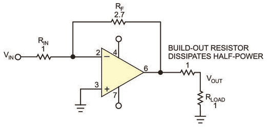
It’s common practice to series-terminate an op amp to match the impedance of the load. This practice causes a 3-dB loss of output power in the termination resistance, however (Figure 1). Newer op amps operating on 3 and 5V have limited output swings, meaning that you should avoid using series-buildout resistors. Instead, you can use a series-feedback circuit to set the output impedance. John Wittman, then a senior staff engineer at GTE Lenkurt Electric Co, introduced this technique more than 40 years ago.
 |
|
| Figure 1. | Using a series-termination resistor equal to the load wastes 3 dB of power and reduces the output swing by one-half. |
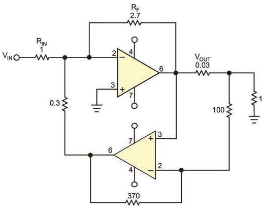
With this technique, you add 6 dB of the reciprocal feedback to set the output impedance, obtaining a return loss of more than 30 dB. You add a series-current- sensing resistor, another op amp, and a limiting resistor (Figure 2). This example shows a high-side sensor and an unbalanced load. The forward amplifier is designed to have twice the needed gain when unloaded. In this example, the open-circuit gain is 2.7, and the input impedance is 1Ω. The input current is 1A, with an input signal of 1V.
 |
|
| Figure 2. | This scheme uses a high-side-current-sense resistor and a second amplifier to set the output impedance to match the load, and it allows almost full output swing. |
To match the amplifier’s 1Ω load, the series-feedback circuitry must divert one-half of the input current from the negative input node of the op amp. The original 1A input current that flows through RF then decreases to 0.5A, meaning that the output voltage is half of the open-circuit voltage. The output impedance is now 1Ω, and the series feedback is 6 dB, allowing you to match the output impedance to the load and still get almost the full voltage swing from the amplifier. You no longer waste half the output power in a series termination. This example uses a current-sense resistance value that is 3% of the output load, so power loss will be 3%. With careful design, you can lower the loss to less than 1%.
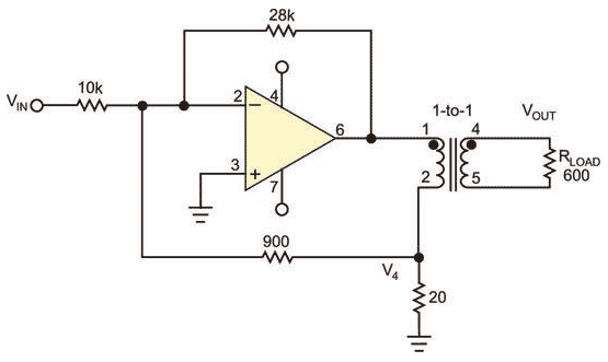
In telecommunications lines, for longitudinal balance, the impedance of both conductors to ground should be the same. Longitudinal balance protects against crosstalk and 60-Hz-induced noise. It is also important at the higher frequencies that DSL (digital-subscriber-line) service uses. Telecom companies commonly use transformers to provide longitudinal balance of 80 to 120 dB. The transformers also isolate transients, such as those due to lightning. You can apply this technique using transformer coupling and low-side current sensing (Figure 3). The design process is still the same, except that just two resistors can provide 6 dB of feedback.
 |
|
| Figure 3. | You can also use low-side sensing of output current to match the output impedance when you have a transformer-coupled output. |
You can formalize the analysis of the circuits using state equations. For the circuit of Figure 2, because the negative input of an op amp is at virtual ground, you can relate input voltage and current by inspection: IIN=(VIN − V−)/1Ω=VIN/1Ω. You can derive a second equation employing the fact that the negative input of an op amp has high impedance, so the currents at that node must add to 0A.
Sum the currents at V−, except you reference the node currents back to the sense resistor, including the 0.3Ω resistor and the 0.03Ω sense resistor: 0=VIN/1Ω+VOUT/2.7Ω+0.37VOUT/ RLOAD. You can express the circuit function in vector and matrix terms: (I)=(ADMITTANCE)×(V). You can also expand for the appropriate states of current:

and then expand for the vector expression of voltage:

Plug these values into the (I)=(ADMITTANCE)×(V) equation and solve for (V):

For the circuit of Figure 2, the forcing function is I1; the input current is 1A. Invert the admittance matrix and then multiply the current vector to find the voltage vector. You can use a Hewlett-Packard (www.hp.com) HP-48 calculator to do the hard work. It yields the result that VIN is 1V and calculates VOUT at −1.35V, one-half the unloaded gain of 2.7. You then repeat the analysis for a load resistance of 1000Ω:

Inverting the (Y) matrix and multiplying it with the I matrix, with I1 of 1A, yields an open-load voltage vector, with VIN equal to 1V and VOUT equal to −2.7V, confirming that the design is correct.
Be careful writing your own equations; two dependent equations can easily lead to an incorrect answer. An HP-48 calculator solves them using the “least-squares” method, but it does not check for a determinant condition of zero to warn you of nonindependent equations. You can use the HP-48 to sum two real matrices to form a complex one. This approach comes in handy when you include reactive elements in the circuit models. If you prefer using a computer rather than a paper napkin, you can also use Spice to analyze this circuit.
Three equations are used to analyze the circuit of Figure 3. You can express the input current as a function of the input resistance: IIN=(VIN − V−)/RIN=VIN/ RIN. As in the previous example, you sum the currents at the amplifier's negative pin to zero, 0=VIN/RIN+VOUT/28 kΩ+(V4 − V−)/900Ω, and then sum the currents at the V4 node: 0=(V4 − V−)/900Ω+(V4 − VOUT)/RLOAD+V4/20Ω.
You express the currents as a vector:
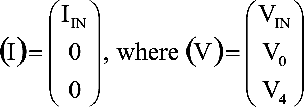
The admittance matrix becomes:
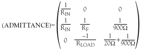
This equation determines (Y), the admittance matrix.
In this case, the input current should be 100 μA, and the load resistance should be 600Ω. Use an HP-48 calculator to invert the admittance matrix and multiply it by the current matrix. The resulting voltage matrix yields an input voltage of 1V, an output voltage of − 1.4V, and a V4 of − 0.05V. Next, set the load to 10,000Ω. Assume that the magnetizing inductance of the transformer is infinite. You then repeat the exercise to check that the output voltage is |2.8V|.
You can match the maximum available signal power from the op amp to the load by changing the transformer turns ratio. Calculate the optimum op-amp signal output impedance to be the peak output swing voltage divided by the maximum peak capability of the op amp.