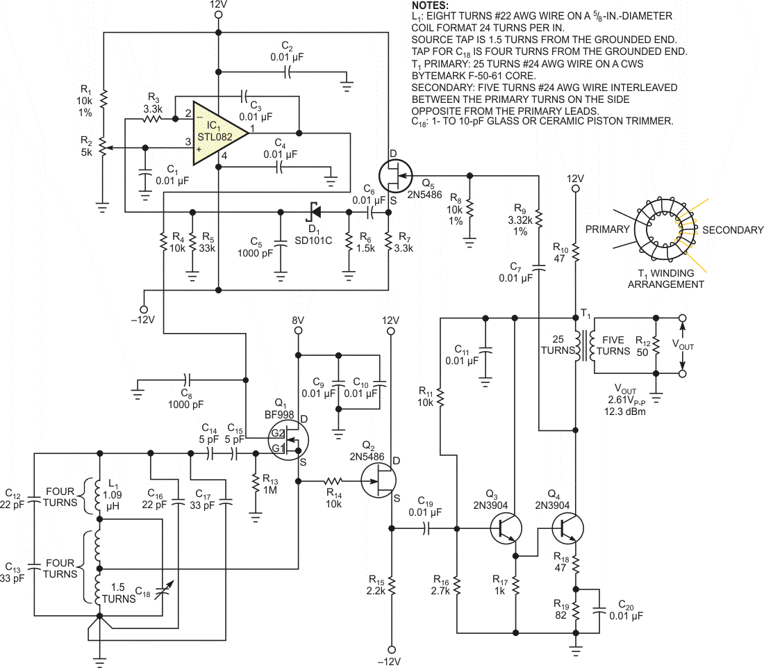
A recent Design Idea described a method for designing simple, high-frequency LC oscillators with few passive components (Reference 1). However, for best results, practical hardware design of a stable oscillator requires more parts and greater complexity. Figure 1 shows a stable, 18-MHz oscillator with automatically leveled output amplitude control and an output buffer that delivers a sine wave with low harmonic content (Reference 2). In addition, this Design Idea replaces the original JFET oscillator with an inexpensive dual-gate MOSFET: an Infineon Technologies BF998, available from DigiKey and other sources.
 |
|
| Figure 1. | This low-distortion, 18-MHz oscillator offers high stability and automatic output-level control. |
The heart of the circuit comprises a Hartley oscillator, Q1. To minimize loading, a 10-kΩ resistor couples the output from Q1's source to the high-input-impedance gate of source follower JFET Q2. In turn, Q2 drives Q3, a BJT (bipolar-junction-transistor) emitter follower, which in turn drives BJT amplifier Q4. Toroidal-core transformer T1 couples 's output to a 50 Ω load, delivering 2.61 V p-p or 12.3 dBm. A Spice-circuit simulation predicts a second-harmonic amplitude of 35 dB below the fundamental. The second harmonic exceeds the amplitudes of all higher order harmonics, and an oscilloscope measurement displays a clean-looking sine wave across the 50 Ω load.
To provide a good termination for the amplifier and still obtain 7.3 dBm (1.47 V p-p) – for example, to drive a diode-ring mixer – you can insert a 50 Ω, 5-dB pad between output transformer T1 and the load. Potentiometer R2 adjusts the RF output level, and, for increased stability, you can replace R2 with a fixed resistive divider built with low-temperature-coefficient, metal-film, fixed resistors. Part of the signal at Q4's collector drives the gate of JFET source follower Q5 through C7 and R9. Diode D1 rectifies the signal, which, after filtering, feeds operational amplifier IC1's inverting input. Resistor R1 and low-temperature-coefficient potentiometer R2 divide the 12 V supply to produce a dc reference voltage for IC1's noninverting input and set the output signal's level. After filtering, IC1's dc output drives Q1's Gate 2 to set the device's gain and thus control RF output.
Connected to the center tap of coil L1, trimmer capacitor C18 allows fine adjustment of the oscillator's frequency. If decreased frequency stability is acceptable, you can replace C18 with a low-cost ceramic trimmer. Piston-type trimmers are rather expensive and less available than ceramic trimmers, but a typical ceramic trimmer exhibits a temperature coefficient that's at least an order of magnitude worse than a piston trimmer's. To operate the oscillator at a frequency other than 18 MHz, multiply the inductance of L1 and the capacitances of C12, C13, C16, C17, and C18 by 18/fOSC2, where fOSC2 is the new frequency in megahertz. Adjust the tap for Q1's source connection so that it remains at about 20% of the winding's total number of turns as counted from the inductor's grounded end.
You can replace the series combinations of C12 and C13 with a 13-pF capacitor, and you can replace C14 and C15 with a 2.5-pF capacitor. If you redesign the circuit for a different frequency, adjust the values of C14 and C15 or their single-capacitor replacement for just enough capacitance to ensure reliable start-up under all anticipated operating conditions. Also, note that using two capacitors for C16 and C17 helps reduce start-up drift, as does using temperature-stable (NP0-characteristic) ceramic-dielectric capacitors for C12 through C17. The buffer amplifier, Q2 through Q4, requires modifications for operation at frequencies above approximately 25 MHz.
A well-regulated external dc source (not shown) provides 12, –12, and 8 V to the circuit. To maintain high stability and remain within Q1's 12 V maximum drain-to-source-voltage rating, the 8 V supply powers only the oscillator. Using the specified components and at a constant ambient temperature of 22 °C, after an initial 10-minute warmup period, the oscillator's frequency drifts at an average rate of –2 to –3 Hz per minute over one hour.
References
- Martínez, H, J Domingo, J Gámiz, and A Grau, "JFETs offer LC oscillators with few components", EDN, Jan 20, 2005, pg 82.
- Reed, DG, editor, "A JFET Hartley VFO," ARRL Handbook for Radio Communications, 82nd Edition, American Radio Relay League, 2005.