PDF, 869 Kb, File published: May 4, 2010
Extract from the document
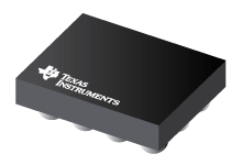
CSD86311W1723
www.ti.com SLPS251 – MAY 2010 Dual N-Channel NexFET™ Power MOSFET
Check for Samples: CSD86311W1723 PRODUCT SUMMARY FEATURES 1 Dual N-Ch MOSFETs
Common Source Configuration
Small Footprint 1.7 mm Г— 2.3 mm
Ultra Low Qg and Qgd
Pb Free
RoHS Compliant
Halogen Free VDS Drain to Source Voltage 25 V Qg Gate Charge Total (4.5V) 3.1 nC Qgd Gate Charge Gate to Drain RDS(on) Drain to Source On Resistance VGS(th) nC
37 mΩ VGS = 4.5V 31 mΩ VGS = 8V 29 mΩ Threshold Voltage 1 V Text Added for Spacing
ORDERING INFORMATION APPLICATIONS 0.33
VGS = 2.5V Battery Management
Battery Protection
DC-DC Converters Device Package Media Qty Ship CSD86311W1723 1.7-mm Г— 2.3-mm
Wafer Level
Package 7-inch reel 3000 Tape and
Reel Text Added for Spacing
ABSOLUTE MAXIMUM RATINGS DESCRIPTION
The device has been designed to deliver the lowest
on resistance and gate charge in the smallest outline
possible with thermal characteristics in an ultra low
profile. Low on resistance and gate charge coupled
with the small footprint and low profile make the …

