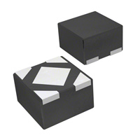
TCR3DM series
TOSHIBA CMOS Linear Integrated Circuit Silicon Monolithic TCR3DM series
300 mA CMOS Low Drop-Out Regulator with inrush current protection circuit
The TCR3DM series are CMOS general-purpose single-output voltage regulators with an on/off control input, featuring low dropout voltage, low output noise voltage and low inrush current. These voltage regulators are available in fixed output voltages between 1.0 V and 4.5 V and capable of driving up to 300 mA. They feature over-current protection, over-temperature protection, Inrush current protection circuit and Auto-discharge function. The TCR3DM series are offered in the ultra small plastic mold package DFN4 (1.0 mm x 1.0 mm; t 0.58 mm). It has a low dropout voltage of 210 mV (2.5 V output, IOUT = 300 mA) with low output BOTTOM VIEW ILLUSTRATION noise voltage of 38 Vrms (2.5 V output) and a load transient DFN4 response of only VOUT = ±80 mV ( IOUT = 1 mA300 mA, COUT Weight : 1.3 mg ( typ.) =1.0 F). As small ceramic input and output capacitors can be used with the TCR3DM series, these devices are ideal for portable applications that require high-density board assembly such as cellular phones. Features Low Drop-Out voltage VIN-VOUT = 210 mV (typ.) at 2.5 V-output, IOUT = 300 mA VIN-VOUT = 270 mV (typ.) at 1.8 V-output, IOUT = 300 mA VIN-VOUT = 490 mV (typ.) at 1.2 V-output, IOUT = 300 mA Low output noise voltage VNO = 38 Vrms (typ.) at 2.5 V-output, IOUT = 10 mA, 10 Hz < f < 100 kHz = = Fast load transient response (VOUT = ±80 mV (typ.) at IOUT = 1 300 mA, COUT =1.0 F ) High ripple rejection ( R.R = 70 dB (typ.) at 2.5V-output, IOUT = 10 mA, f =1kHz ) Over-current protection Over-temperature protection Inrush current protection circuit Auto-discharge function Pull down connection between CONTROL and GND Ceramic capacitors can be used ( CIN = 1.0F, COUT =1.0 F ) Ultra small package DFN4 (1.0 mm x 1.0 mm ; t 0.58 mm ) Start of commercial production 2013-03 1 2014-07-09 TCR3DM series
Absolute Maximum Ratings (Ta = 25°C)
Characteristics Input voltage Control voltage Output voltage Output current Power dissipation Operation temperature range Junction temperature Storage temperature range Symbol VIN VCT VOUT IOUT PD Topr Tj Tstg 420 Rating 6.0 -0.3 to 6.0 -0.3 to VIN + 0.3 300 (Note1) Unit V V V mA mW °C °C °C -40 to 85 150 -55 to 150 Note: Using continuously under heavy loads (e.g. the application of high temperature/current/voltage and the significant change in temperature, etc.) may cause this product to decrease in the reliability significantly even if the operating conditions (i.e. operating temper …

