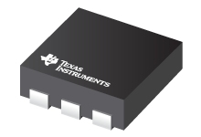
Datasheet Texas Instruments TPS61170DRVRG4
| Manufacturer | Texas Instruments |
| Series | TPS61170 |
| Part Number | TPS61170DRVRG4 |

1.2A Switch, High Voltage Boost Converter in 2x2mm QFN Package 6-WSON -40 to 85
Datasheets
TPS61170 1.2-A High-Voltage Boost Converter in 2-mm x 2-mm2 QFN Package datasheet
PDF, 1.2 Mb, Revision: D, File published: Dec 18, 2014
Extract from the document
Prices
Status
| Lifecycle Status | Active (Recommended for new designs) |
| Manufacture's Sample Availability | Yes |
Packaging
| Pin | 6 |
| Package Type | DRV |
| Industry STD Term | WSON |
| JEDEC Code | S-PDSO-N |
| Package QTY | 3000 |
| Carrier | LARGE T&R |
| Device Marking | BZS |
| Width (mm) | 2 |
| Length (mm) | 2 |
| Thickness (mm) | .75 |
| Pitch (mm) | .65 |
| Max Height (mm) | .8 |
| Mechanical Data | Download |
Parametrics
| Duty Cycle(Max) | 93 % |
| Iq(Typ) | 2.3 mA |
| Operating Temperature Range | -40 to 85 C |
| Package Group | WSON |
| Rating | Catalog |
| Regulated Outputs | 1 |
| Special Features | Enable,Light Load Efficiency |
| Switch Current Limit(Min) | 0.96 A |
| Switch Current Limit(Typ) | 1.2 A |
| Switching Frequency(Max) | 1200 kHz |
| Switching Frequency(Min) | 1000 kHz |
| Type | Converter |
| Vin(Max) | 18 V |
| Vin(Min) | 3 V |
| Vout(Max) | 38 V |
| Vout(Min) | 3 V |
Eco Plan
| RoHS | Compliant |
Design Kits & Evaluation Modules
- Evaluation Modules & Boards: TPS61170EVM-316
TPS61170EVM-316 Evaluation Module
Lifecycle Status: Active (Recommended for new designs) - Evaluation Modules & Boards: TPS61170EVM-280
TPS61170 12V Input, 24V Output, 0.34A Evaluation Module
Lifecycle Status: Active (Recommended for new designs)
Application Notes
- Load Disconnect for the TPS61170 (Rev. A)PDF, 80 Kb, Revision: A, File published: Mar 14, 2011
- Designing DC/DC converters based on SEPIC topologyPDF, 705 Kb, File published: Oct 22, 2008
- Simple open-circuit protection for boost converters in LED driver applicationsPDF, 246 Kb, File published: Sep 25, 2012
- How to Design a Boost Converter With the TPS61170 (Rev. C)PDF, 400 Kb, Revision: C, File published: Jun 6, 2012
- How to Design a SEPIC Converter With the TPS61175PDF, 586 Kb, File published: Jun 12, 2009
When a dc/dc converter providing a regulated output voltage between the minimum and maximum input voltage is required, neither a single buck or a boost converter can provide the output voltage. However, a boost converter integrated circuit (IC) can be configured to drive a single-ended, primary-inductor converter (SEPIC) power stage and provide an output voltage that is between the input voltage e - Input Current Limit Solution for USB-Supplied Power SystemPDF, 666 Kb, File published: Aug 3, 2017
- Description Compensating the Current Mode Boost Control LoopPDF, 411 Kb, File published: Dec 9, 2010
- Compensating and measuring the DC/DC converter loop that powers a high-power LEDPDF, 618 Kb, File published: Oct 22, 2008
- Coupled inductors broaden DC/DC converter usagePDF, 140 Kb, File published: Aug 11, 2010
- Extending the Input Voltage Range of the TPS6116x/8x/9x WLED DriversPDF, 124 Kb, File published: Aug 12, 2009
The TPS6116x, TPS6118x and TPS6119x WLED driver and TPS6117x boost converter integrated circuits (IC) can operate with different input voltages, one powering the IC itself and the other powering the boost power stage. This application report explains various options on how to use the WLED drivers with split power rails. This allows these LED drivers to be used in applications where the available - Design of UVLO for LM27313 (Rev. B)PDF, 142 Kb, Revision: B, File published: Apr 8, 2014
- 3Q 2010 Issue Analog Applications JournalPDF, 1.5 Mb, File published: Aug 11, 2010
- 4Q 2012 Issue Analog Applications JournalPDF, 3.3 Mb, File published: Sep 25, 2012
- Q4 2008 Issue Analog Applications JournalPDF, 1.5 Mb, File published: Oct 22, 2008
- Design considerations for a resistive feedback divider in a DC/DC converterPDF, 393 Kb, File published: Apr 26, 2012
- Basic Calculation of a Boost Converter's Power Stage (Rev. C)PDF, 186 Kb, Revision: C, File published: Jan 8, 2014
This application note gives the equations to calculate the power stage of a boost converter built with an IC with integrated switch and operating in continuous conduction mode. It is not intended to give details on the functionality of a boost converter (see Reference 1) or how to compensate a converter. See the references at the end of this document if more detail is needed. - Optimizing Transient Response of Internally Compensated DC-DC Converters (Rev. A)PDF, 1.1 Mb, Revision: A, File published: May 11, 2015
- Extending the Soft Start Time Without a Soft Start Pin (Rev. B)PDF, 387 Kb, Revision: B, File published: Jun 15, 2017
- QFN and SON PCB Attachment (Rev. B)PDF, 821 Kb, Revision: B, File published: Aug 24, 2018
- IQ: What it is what it isn’t and how to use itPDF, 198 Kb, File published: Jun 17, 2011
- Performing Accurate PFM Mode Efficiency Measurements (Rev. A)PDF, 418 Kb, Revision: A, File published: Dec 11, 2018
When performing measurements on DC-DC converters using pulse frequency modulation(PFM)or any power save mode proper care must be taken to ensure that the measurements are accurate. An accurate PFM mode efficiency measurement is critical for systems which require high efficiency at low loads such as in smart home systems tablets wearables and metering.
Model Line
Series: TPS61170 (4)
- TPS61170DRVR TPS61170DRVRG4 TPS61170DRVT TPS61170DRVTG4
Manufacturer's Classification
- Semiconductors > Power Management > Non-isolated DC/DC Switching Regulator > Step-Up (Boost) > Boost Converter (Integrated Switch)
