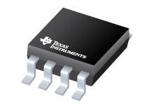
Datasheet Texas Instruments TLV2545CDGK
| Manufacturer | Texas Instruments |
| Series | TLV2545 |
| Part Number | TLV2545CDGK |

12-Bit, 200 kSPS ADC, Ser. Out, TMS320 Compatible (up to 10MHz), Single Ch. Pseudo-Differential 8-VSSOP 0 to 70
Datasheets
2.7 V to 5.5 V Low-Power 12-Bit 140/200 KSPS, Serial Analog-To-Digital Converter datasheet
PDF, 1.2 Mb, Revision: E, File published: Apr 12, 2010
Extract from the document
Prices
Status
| Lifecycle Status | Active (Recommended for new designs) |
| Manufacture's Sample Availability | No |
Packaging
| Pin | 8 |
| Package Type | DGK |
| Industry STD Term | VSSOP |
| JEDEC Code | R-PDSO-G |
| Package QTY | 80 |
| Carrier | TUBE |
| Device Marking | AHD |
| Width (mm) | 3 |
| Length (mm) | 3 |
| Thickness (mm) | .97 |
| Pitch (mm) | .65 |
| Max Height (mm) | 1.07 |
| Mechanical Data | Download |
Parametrics
| # Input Channels | 1 |
| Analog Voltage AVDD(Max) | 5.5 V |
| Analog Voltage AVDD(Min) | 2.7 V |
| Architecture | SAR |
| Digital Supply(Max) | 5.5 V |
| Digital Supply(Min) | 2.7 V |
| INL(Max) | 1 +/-LSB |
| Input Range(Max) | 5.5 V |
| Input Type | Pseudo-Differential |
| Integrated Features | Oscillator |
| Interface | SPI |
| Multi-Channel Configuration | N/A |
| Operating Temperature Range | 0 to 70,-40 to 85 C |
| Package Group | VSSOP |
| Package Size: mm2:W x L | 8VSSOP: 15 mm2: 4.9 x 3(VSSOP) PKG |
| Power Consumption(Typ) | 2.8 mW |
| Rating | Catalog |
| Reference Mode | Ext |
| Resolution | 12 Bits |
| SINAD | 72 dB |
| SNR | 72 dB |
| Sample Rate (max) | 200kSPS SPS |
| Sample Rate(Max) | 0.2 MSPS |
| THD(Typ) | -84 dB |
Eco Plan
| RoHS | Compliant |
Design Kits & Evaluation Modules
- Evaluation Modules & Boards: TLV2545EVM
TLV2545 Evaluation Module
Lifecycle Status: Obsolete (Manufacturer has discontinued the production of the device) - Evaluation Modules & Boards: 5-6KINTERFACE
5-6K Interface Evaluation Module
Lifecycle Status: Active (Recommended for new designs)
Application Notes
- Determining Minimum Acquisition Times for SAR ADCs, part 1 (Rev. A)PDF, 227 Kb, Revision: A, File published: Nov 10, 2010
This application report analyzes a simple method for calculating minimum acquisition times for successive-approximation register analog-to-digital converters (SAR ADCs). The input structure of the ADC is examined along with the driving circuit. The voltage on the sampling capacitor is then determined for the case when a step function is applied to the input of the driving circuit. Three different - Determining Minimum Acquisition Times for SAR ADCs, part 2PDF, 215 Kb, File published: Mar 17, 2011
The input structure circuit of a successive-approximation register analog-to-digital converter (SAR ADC) incombination with the driving circuit forms a transfer function that can be used to determine minimum acquisition times for different types of applied input signals. This application report, which builds on Determining Minimum Acquisition Times for SAR ADCs When a Step Function is Applied to
Model Line
Series: TLV2545 (3)
- TLV2545CDGK TLV2545ID TLV2545IDGK
Manufacturer's Classification
- Semiconductors > Data Converters > Analog-to-Digital Converters (ADCs) > Precision ADCs (<=10MSPS)
