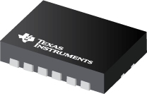
Datasheet Texas Instruments TPS61096DSST
| Manufacturer | Texas Instruments |
| Series | TPS61096 |
| Part Number | TPS61096DSST |

28-V Output Voltage Boost Converter with 1-ВµA Quiescent Current 12-WSON -40 to 85
Datasheets
Prices
Status
| Lifecycle Status | Active (Recommended for new designs) |
| Manufacture's Sample Availability | No |
Packaging
| Pin | 12 |
| Package Type | DSS |
| Industry STD Term | WSON |
| JEDEC Code | R-PDSO-N |
| Package QTY | 250 |
| Carrier | SMALL T&R |
| Device Marking | S61096 |
| Width (mm) | 3 |
| Length (mm) | 2 |
| Thickness (mm) | .75 |
| Pitch (mm) | .5 |
| Max Height (mm) | .8 |
| Mechanical Data | Download |
Parametrics
| Approx. Price (US$) | 0.80 | 1ku |
| Duty Cycle(Max)(%) | 90 |
| Iq(Typ)(mA) | 0.001 |
| Operating Temperature Range(C) | -40 to 85 |
| Package Group | WSON |
| Rating | Catalog |
| Regulated Outputs(#) | 1 |
| Special Features | Adjustable Current Limit Enable Light Load Efficiency |
| Switch Current Limit(Min)(A) | 0.4 |
| Switch Current Limit(Typ)(A) | 0.5 |
| Type | Converter |
| Vin(Max)(V) | 5.5 |
| Vin(Min)(V) | 1.8 |
| Vout(Max)(V) | 28 |
| Vout(Min)(V) | 4.5 |
Eco Plan
| RoHS | Compliant |
| Pb Free | Yes |
Design Kits & Evaluation Modules
- Evaluation Modules & Boards: TPS61096EVM-787
Evaluation Board for TPS61096 28-V Output Voltage Boost Converter with Ultra-Low Quiescent Current
Lifecycle Status: Active (Recommended for new designs)
Application Notes
- AN-1112 DSBGA Wafer Level Chip Scale Package (Rev. AG)PDF, 13.7 Mb, Revision: AG, File published: Aug 12, 2015
- Automated Frequency Response AnalyzerPDF, 939 Kb, File published: Oct 9, 2013
This application report discusses a new method of doing stability Analysis testing by using basic labequipment, while not requiring any specific instruments. - Minimizing Ringing at the Switch Node of a Boost ConverterPDF, 201 Kb, File published: Sep 15, 2006
The application report explains how to use proper board layout and/or a snubber to reduce high-frequency ringing at the switch node of a boost converter. - Design considerations for a resistive feedback divider in a DC/DC converterPDF, 393 Kb, File published: Apr 26, 2012
- Basic Calculation of a Boost Converter's Power Stage (Rev. C)PDF, 186 Kb, Revision: C, File published: Jan 8, 2014
This application note gives the equations to calculate the power stage of a boost converter built with an IC with integrated switch and operating in continuous conduction mode. It is not intended to give details on the functionality of a boost converter (see Reference 1) or how to compensate a converter. See the references at the end of this document if more detail is needed. - Optimizing Transient Response of Internally Compensated DC-DC Converters (Rev. A)PDF, 1.1 Mb, Revision: A, File published: May 11, 2015
- IQ: What it is what it isn’t and how to use itPDF, 198 Kb, File published: Jun 17, 2011
- Performing Accurate PFM Mode Efficiency Measurements (Rev. A)PDF, 418 Kb, Revision: A, File published: Dec 11, 2018
When performing measurements on DC-DC converters using pulse frequency modulation(PFM)or any power save mode proper care must be taken to ensure that the measurements are accurate. An accurate PFM mode efficiency measurement is critical for systems which require high efficiency at low loads such as in smart home systems tablets wearables and metering.
Model Line
Series: TPS61096 (2)
- TPS61096DSSR TPS61096DSST
Manufacturer's Classification
- Semiconductors > Power Management > Non-isolated DC/DC Switching Regulator > Step-Up (Boost) > Boost Converter (Integrated Switch)
