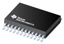
Datasheet Texas Instruments TLC5540INSLE
| Manufacturer | Texas Instruments |
| Series | TLC5540 |
| Part Number | TLC5540INSLE |

8-Bit, 40 MSPS ADC Single Ch., Internal S&H, Low Power 24-SO
Datasheets
TLC5540: 8-Bit High-Speed Analog-to-Digital Converter datasheet
PDF, 867 Kb, Revision: D, File published: Apr 19, 2004
Extract from the document
Prices
Status
| Lifecycle Status | Obsolete (Manufacturer has discontinued the production of the device) |
| Manufacture's Sample Availability | No |
Packaging
| Pin | 24 |
| Package Type | NS |
| Industry STD Term | SOP |
| JEDEC Code | R-PDSO-G |
| Width (mm) | 5.3 |
| Length (mm) | 15 |
| Thickness (mm) | 1.95 |
| Pitch (mm) | 1.27 |
| Max Height (mm) | 2 |
| Mechanical Data | Download |
Replacements
| Replacement | TLC5540INSR |
| Replacement Code | S |
Parametrics
| # Input Channels | 1 |
| Analog Input BW(MHz) | 75 |
| Approx. Price (US$) | 2.64 | 1ku |
| Architecture | Flash |
| DNL(Max)(+/-LSB) | 1 |
| ENOB(Bits) | 6.8 |
| INL(Max)(+/-LSB) | 1 |
| Input Buffer | No |
| Input Range | +2V |
| Interface | Parallel CMOS |
| Operating Temperature Range(C) | -40 to 85 0 to 70 |
| Package Group | SO |
| Package Size: mm2:W x L (PKG) | 24TSSOP: 50 mm2: 6.4 x 7.8(TSSOP) |
| Power Consumption(Typ)(mW) | 85 |
| Rating | Catalog |
| Reference Mode | Ext |
| Resolution(Bits) | 8 |
| SFDR(dB) | 42 |
| SNR(dB) | 44 |
| Sample Rate(Max)(MSPS) | 40 |
Eco Plan
| RoHS | Not Compliant |
| Pb Free | No |
Design Kits & Evaluation Modules
- Evaluation Modules & Boards: TLC5540EVM
TLC5540 Evaluation Module
Lifecycle Status: Active (Recommended for new designs) - Evaluation Modules & Boards: TSW2200EVM
TSW2200EVM: Low Cost Portable Power Supply
Lifecycle Status: Active (Recommended for new designs)
Application Notes
- Interfacing the TLC5540 Analog To Digital Converter to the TMS320C203-80 DSPPDF, 763 Kb, File published: Mar 1, 1998
CMOS analog-to-digital converters (ADCs) are used as basic building blocks in many types of data acquisition systems.This application report describes the interface between the high-speed Texas Instruments (TI?TLC5540 8-bit parallel-output ADC and the TI TMS320C203-80 digital signal processor (DSP). The 8-bit resolution ADC can operate at a rate of up to 40MSa/s (megasamples per second). On-ch - Interfacing A/D Converters TLC5540/10 to the DSKplus DSP Starter Kit TMS320C54xPDF, 206 Kb, File published: Apr 1, 1997
This Application Note describes the construction of a test circuit using the A/D converters TLC5540 and TLC5510, and alternative ways of interfacing these converters to the DSKplus DSP starter kit TMS320C54x. Details are given of the test circuit of the TLC5540/10 and of the interface, and the programming of the digital signal processor TMS320C54x is also described. - CDCE62005 as Clock Solution for High-Speed ADCsPDF, 805 Kb, File published: Sep 4, 2008
TI has introduced a family of devices well-suited to meet the demands for high-speed ADC devices such as the ADS5527 which is capable of sampling up to 210 MSPS. To realize the full potential of these high-performance products it is imperative to provide a low phase noise clock source. The CDCE62005 clock synthesizer chip offers a real-world clocking solution to meet these stringent requirements - Smart Selection of ADC/DAC Enables Better Design of Software-Defined RadioPDF, 376 Kb, File published: Apr 28, 2009
This application report explains different aspects of selecting analog-to-digital and digital-to-analog data converters for Software-Defined Radio (SDR) applications. It also explains how ADS61xx ADCs and the DAC5688 from Texas Instruments fit properly for SDR designs. - Driving High-Speed ADCs: Circuit Topologies and System-Level Parameters (Rev. A)PDF, 327 Kb, Revision: A, File published: Sep 10, 2010
This application report discusses the performance-related aspects of passive and active interfaces at the analog input of high-speed pipeline analog-to-digital converters (ADCs). The report simplifies the many possibilities into two main categories: passive and active interface circuits. The first section of the report gives an overview of equivalent models of buffered and unbuffered ADC input cir - Phase Noise Performance and Jitter Cleaning Ability of CDCE72010PDF, 2.3 Mb, File published: Jun 2, 2008
This application report presents phase noise data taken on the CDCE72010 jitter cleaner and synchronizer PLL device. The phase noise performance of the CDCE72010 depends on the phase noise of the reference clock VCXO clock and the CDCE72010 itself. This application report shows the phase noise performance at several of the most popular CDMA frequencies. This data helps the user to choose the rig - CDCE72010 as a Clocking Solution for High-Speed Analog-to-Digital ConvertersPDF, 424 Kb, File published: Jun 8, 2008
Texas Instruments has recently introduced a family of devices suitable to meet the demands of high-speed high-IF sampling analog-to-digital converters (ADCs) such as the ADS5483 which is capable of sampling up to 135 MSPS. To realize the full potential of these high-performance devices the system must provide an extremely low phase noise clock source. The CDCE72010 clock synthesizer chip offers
Model Line
Series: TLC5540 (8)
Manufacturer's Classification
- Semiconductors > Data Converters > Analog to Digital Converter > High Speed ADC (>10MSPS)
