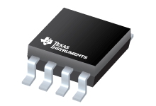
Datasheet Texas Instruments TPS61085PW
| Manufacturer | Texas Instruments |
| Series | TPS61085 |
| Part Number | TPS61085PW |

18.5V, 2A, 650kHz / 1.2MHz Step-Up DC-DC Converter w/ Forced PWM Mode 8-TSSOP -40 to 85
Datasheets
TPS61085 650-kHz,1.2-MHz, 18.5-V Step-Up DC-DC Converter datasheet
PDF, 1.4 Mb, Revision: B, File published: Dec 15, 2014
Extract from the document
Prices
Status
| Lifecycle Status | Active (Recommended for new designs) |
| Manufacture's Sample Availability | No |
Packaging
| Pin | 8 |
| Package Type | PW |
| Industry STD Term | TSSOP |
| JEDEC Code | R-PDSO-G |
| Package QTY | 150 |
| Carrier | TUBE |
| Device Marking | 61085 |
| Width (mm) | 4.4 |
| Length (mm) | 3 |
| Thickness (mm) | 1 |
| Pitch (mm) | .65 |
| Max Height (mm) | 1.2 |
| Mechanical Data | Download |
Parametrics
| Duty Cycle(Max) | 90 % |
| Iq(Typ) | 0.07 mA |
| Operating Temperature Range | -40 to 85 C |
| Package Group | TSSOP |
| Rating | Catalog |
| Regulated Outputs | 1 |
| Special Features | Frequency Synchronization |
| Switch Current Limit(Min) | 2 A |
| Switch Current Limit(Typ) | 2.6 A |
| Switching Frequency(Max) | 1500 kHz |
| Switching Frequency(Min) | 480 kHz |
| Type | Converter |
| Vin(Max) | 6 V |
| Vin(Min) | 2.3 V |
| Vout(Max) | 18.5 V |
| Vout(Min) | 2.8 V |
Eco Plan
| RoHS | Compliant |
Design Kits & Evaluation Modules
- Evaluation Modules & Boards: TPS61085EVM-355
TPS61085 Evaluation Module
Lifecycle Status: Active (Recommended for new designs)
Application Notes
- Low Cost 1W Isolated Power Supply Solution with TPS61085PDF, 175 Kb, File published: Jun 26, 2012
- AN-2020 Thermal Design By Insight, Not Hindsight (Rev. C)PDF, 568 Kb, Revision: C, File published: Apr 23, 2013
This application report provides an in-depth discussion of thermal design. - Minimizing Ringing at the Switch Node of a Boost ConverterPDF, 201 Kb, File published: Sep 15, 2006
The application report explains how to use proper board layout and/or a snubber to reduce high-frequency ringing at the switch node of a boost converter. - Design considerations for a resistive feedback divider in a DC/DC converterPDF, 393 Kb, File published: Apr 26, 2012
- Basic Calculation of a Boost Converter's Power Stage (Rev. C)PDF, 186 Kb, Revision: C, File published: Jan 8, 2014
This application note gives the equations to calculate the power stage of a boost converter built with an IC with integrated switch and operating in continuous conduction mode. It is not intended to give details on the functionality of a boost converter (see Reference 1) or how to compensate a converter. See the references at the end of this document if more detail is needed. - PowerPAD Thermally Enhanced Package (Rev. H)PDF, 983 Kb, Revision: H, File published: Jul 6, 2018
- Understanding the Absolute Maximum Ratings of the SW Node (Rev. A)PDF, 755 Kb, Revision: A, File published: Jan 13, 2012
- Extending the Soft Start Time Without a Soft Start Pin (Rev. B)PDF, 387 Kb, Revision: B, File published: Jun 15, 2017
- IQ: What it is what it isn’t and how to use itPDF, 198 Kb, File published: Jun 17, 2011
- Performing Accurate PFM Mode Efficiency Measurements (Rev. A)PDF, 418 Kb, Revision: A, File published: Dec 11, 2018
When performing measurements on DC-DC converters using pulse frequency modulation(PFM)or any power save mode proper care must be taken to ensure that the measurements are accurate. An accurate PFM mode efficiency measurement is critical for systems which require high efficiency at low loads such as in smart home systems tablets wearables and metering.
Model Line
Series: TPS61085 (9)
Manufacturer's Classification
- Semiconductors > Power Management > Non-isolated DC/DC Switching Regulator > Step-Up (Boost) > Boost Converter (Integrated Switch)
