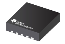
Datasheet Texas Instruments TPS62421DRCR
| Manufacturer | Texas Instruments |
| Series | TPS62421 |
| Part Number | TPS62421DRCR |

2.25MHz 600mA/1000mA Dual Step Down Converter In Small 3x3mm QFN Package 10-VSON -40 to 85
Datasheets
TPS6242x 2.25-MHz 600-mA and 1000-mA Dual Step-Down Converter in Small 3-mm Г— 3-mm VSON Package datasheet
PDF, 1.6 Mb, Revision: D, File published: Jul 31, 2015
Extract from the document
Prices
Status
| Lifecycle Status | Active (Recommended for new designs) |
| Manufacture's Sample Availability | Yes |
Packaging
| Pin | 10 |
| Package Type | DRC |
| Industry STD Term | VSON |
| JEDEC Code | S-PDSO-N |
| Package QTY | 3000 |
| Carrier | LARGE T&R |
| Device Marking | QTQ |
| Width (mm) | 3 |
| Length (mm) | 3 |
| Thickness (mm) | .9 |
| Pitch (mm) | .5 |
| Max Height (mm) | 1 |
| Mechanical Data | Download |
Parametrics
| Control Mode | Voltage Mode |
| Duty Cycle(Max) | 100 % |
| Iout(Max) | 0.6 A |
| Iq(Typ) | 0.032 mA |
| Operating Temperature Range | -40 to 85 C |
| Package Group | VSON |
| Rating | Catalog |
| Regulated Outputs | 2 |
| Special Features | Dynamic Voltage Scaling,Enable,Light Load Efficiency,Synchronous Rectification |
| Switching Frequency(Max) | 2500 kHz |
| Switching Frequency(Min) | 2000 kHz |
| Type | Converter |
| Vin(Max) | 6 V |
| Vin(Min) | 2.5 V |
| Vout(Max) | 1.8 V |
| Vout(Min) | 1.2 V |
Eco Plan
| RoHS | Compliant |
Application Notes
- Output Voltage Selection for the TPS62400 Family of Buck ConvertersPDF, 58 Kb, File published: Sep 20, 2006
This application report explains how to determine the output voltage of the TPS62400 after power up and the software adjustable range of voltages - Power Solution using a Dual DCDC Converter and a LDO (Rev. A)PDF, 174 Kb, Revision: A, File published: Mar 25, 2010
- Power for TMS320C5504/05 (Rev. A)PDF, 204 Kb, Revision: A, File published: Apr 23, 2010
- TMS320F28xx and TMS320F28xxx DSP Power Reference Design (Rev. A)PDF, 125 Kb, Revision: A, File published: Apr 10, 2008
This reference design takes into account the voltage, current, and start-up requirements of the TMS320F280x Digital Signal Processor (DSP) families. The operating input voltage ranges from 3.4 V to 6 V. This design is a high-efficiency solution that provides two voltage rails (1.8-V core supply and 3.3-V I/O supply) and an active-low reset signal to the DSP. This design can be easily adapted to fi - Optimizing Transient Response of Internally Compensated DC-DC Converters (Rev. A)PDF, 1.1 Mb, Revision: A, File published: May 11, 2015
- Five steps to a great PCB layout for a step-down converterPDF, 162 Kb, File published: Jan 29, 2015
- Understanding the Absolute Maximum Ratings of the SW Node (Rev. A)PDF, 755 Kb, Revision: A, File published: Jan 13, 2012
- Testing tips for applying external power to supply outputs without an input voltPDF, 110 Kb, File published: Oct 24, 2016
- Basic Calculation of a Buck Converter's Power Stage (Rev. B)PDF, 202 Kb, Revision: B, File published: Aug 17, 2015
- Extending the Soft Start Time Without a Soft Start Pin (Rev. B)PDF, 387 Kb, Revision: B, File published: Jun 15, 2017
- QFN and SON PCB Attachment (Rev. B)PDF, 821 Kb, Revision: B, File published: Aug 24, 2018
- IQ: What it is what it isn’t and how to use itPDF, 198 Kb, File published: Jun 17, 2011
- Performing Accurate PFM Mode Efficiency Measurements (Rev. A)PDF, 418 Kb, Revision: A, File published: Dec 11, 2018
When performing measurements on DC-DC converters using pulse frequency modulation(PFM)or any power save mode proper care must be taken to ensure that the measurements are accurate. An accurate PFM mode efficiency measurement is critical for systems which require high efficiency at low loads such as in smart home systems tablets wearables and metering.
Model Line
Series: TPS62421 (2)
- TPS62421DRCR TPS62421DRCT
Manufacturer's Classification
- Semiconductors > Power Management > Non-isolated DC/DC Switching Regulator > Step-Down (Buck) > Buck Converter (Integrated Switch)
