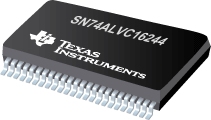
16-Bit Buffer/Driver With 3-State Outputs 48-SSOP -40 to 85
PDF, 378 Kb, Revision: B, File published: Feb 23, 2005
Simultaneous-switching noise can generate and propagate glitches in electronic systems. Therefore, system designers are faced with challenges to minimize simultaneous-switching noise, while increasing switching speed and improving signal quality. This report presents the performance of different TI logic devices under various simultaneous-switching conditions. Factors such as the number of bits sw
PDF, 43 Kb, File published: Aug 3, 1998
The PC100 standard establishes design parameters for the PC SDRAM DIMM that is designed to operate at 100 MHz. The 168-pin, 8-byte, registered SDRAM DIMM is a JEDEC-defined device (JC-42.5-96-146A). Some of the defined signal paths include data signals, address signals, and control signals. This application report discusses the SN74ALVC16835 18-bit universal bus driver that is available from T
PDF, 96 Kb, Revision: A, File published: May 13, 1998
Design of high-performance personal computer (PC) systems that are capable of meeting the needs imposed by modern operating systems and software includes the use of large banks of SDRAMs on DIMMs (see Figure 1).To meet the demands of stable functionality over the broad spectrum of operating environments, meet system timing needs, and to support data integrity, the loads presented by the large
PDF, 895 Kb, Revision: B, File published: May 22, 2002
TI?s 56-ball MicroStar Jr.E package registered under JEDEC MO-225 has demonstrated through modeling and experimentation that it is an optimal solution for reducing inductance and capacitance improving thermal performance and minimizing board area usage in integrated bus functions. Multiple functions released in the 56-ball MicroStar Jr.E package have superior performance characteristics compa
PDF, 154 Kb, Revision: A, File published: Sep 8, 1999
In the last few years the trend toward reducing supply voltage (VCC) has continued as reflected in an additional specification of 2.5-V VCC for the AVC ALVT ALVC LVC LV and the CBTLV families.In this application report the different logic levels at VCC of 5 V 3.3 V 2.5 V and 1.8 V are compared. Within the report the possibilities for migration from 5-V logic and 3.3-V logic families

