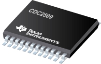
Datasheet Texas Instruments CDC2509PWRG4
| Manufacturer | Texas Instruments |
| Series | CDC2509 |
| Part Number | CDC2509PWRG4 |

3.3-V Phase-Lock Loop Clock Driver With 3-State Outputs 24-TSSOP
Datasheets
CDC2509: 3.3-V Phase-Lock Loop Clock Driver (Rev. C)
PDF, 614 Kb, Revision: C, File published: Dec 2, 2004
Prices
Status
| Lifecycle Status | NRND (Not recommended for new designs) |
| Manufacture's Sample Availability | No |
Packaging
| Pin | 24 |
| Package Type | PW |
| Industry STD Term | TSSOP |
| JEDEC Code | R-PDSO-G |
| Package QTY | 2000 |
| Carrier | LARGE T&R |
| Device Marking | CK2509 |
| Width (mm) | 4.4 |
| Length (mm) | 7.8 |
| Thickness (mm) | 1 |
| Pitch (mm) | .65 |
| Max Height (mm) | 1.2 |
| Mechanical Data | Download |
Eco Plan
| RoHS | Compliant |
| Pb Free | Yes |
Application Notes
- Understanding the Differences Between CDC2509x/10x DevicesPDF, 65 Kb, File published: Jan 8, 1999
This application note provides information concerning the various revisions of the TI CDC2509/10 family of devices. In addition, it will assist designers with new and existing designs. Phase error information, both slope and absolute value, is provided to assist in the tuning process. Furthermore, a table summarizes important parameters for choosing the correct PLL. The table contains capacitance - High Speed Clock Distribution Design Techniques for CDC 509/516/2509/2510/2516 (Rev. A)PDF, 109 Kb, Revision: A, File published: Sep 23, 1998
The memory bandwidth of high performance microprocessors is increasing at a rapid rate and the future memory bandwidth requirements are expected to keep increasing. The bandwidth requirements of RAM will be satisfied in the near term by using Synchronous DRAM. The need to drive multiple DRAM chips at high speeds with low skew necessitates the use of clock distribution devices with Phase Locked Loo
Model Line
Series: CDC2509 (2)
- CDC2509PWR CDC2509PWRG4
Manufacturer's Classification
- Semiconductors > Clock and Timing > Clock Buffers > Zero Delay Buffers
