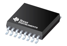
Datasheet Texas Instruments CDCE925PWR
| Manufacturer | Texas Instruments |
| Series | CDCE925 |
| Part Number | CDCE925PWR |

Programmable 2-PLL VCXO Clock Synthesizer with 2.5-V or 3.3-V LVCMOS Outputs 16-TSSOP -40 to 85
Datasheets
CDCE(L)925: Flexible Low Power LVCMOS Clock Generator With SSC Support for EMI Reduction datasheet
PDF, 1.5 Mb, Revision: I, File published: Oct 27, 2016
Extract from the document
Prices
Status
| Lifecycle Status | Active (Recommended for new designs) |
| Manufacture's Sample Availability | No |
Packaging
| Pin | 16 |
| Package Type | PW |
| Industry STD Term | TSSOP |
| JEDEC Code | R-PDSO-G |
| Package QTY | 2000 |
| Carrier | LARGE T&R |
| Device Marking | CDCE925 |
| Width (mm) | 4.4 |
| Length (mm) | 5 |
| Thickness (mm) | 1 |
| Pitch (mm) | .65 |
| Max Height (mm) | 1.2 |
| Mechanical Data | Download |
Parametrics
| Divider Ratio | Universal |
| Function | Clock Synthesizer |
| Input Level | Crystal,LVCMOS |
| Jitter-Peak to Peak(P-P) or Cycle to Cycle | 60 ps C-C |
| Number of Outputs | 5 |
| Operating Temperature Range | -40 to 85 C |
| Output Frequency(Max) | 230 MHz |
| Output Level | LVCMOS |
| Output Skew | 150 ps |
| Package Group | TSSOP |
| Package Size: mm2:W x L | 16TSSOP: 32 mm2: 6.4 x 5(TSSOP) PKG |
| Programmability | EEPROM |
| Rating | Catalog |
| Special Features | Integrated EEPROM,Multiplier/Divider,Spread Spectrum Clocking (SSC) |
| VCC | 1.8 V |
| VCC Core | 1.8 V |
| VCC Out | 3.3, 2.5 V |
Eco Plan
| RoHS | Compliant |
Design Kits & Evaluation Modules
- Evaluation Modules & Boards: CDCE925PERF-EVM
CDCE925 Performance Evaluation Module
Lifecycle Status: Active (Recommended for new designs) - Evaluation Modules & Boards: CDCEL9XXPROGEVM
CDCE(L)949 Family EEPROM Programming Board
Lifecycle Status: Active (Recommended for new designs) - Evaluation Modules & Boards: DP83822EVM
DP83822 10/100 Mbps Ethernet PHY Evaluation Module
Lifecycle Status: Active (Recommended for new designs)
Application Notes
- General I2C / EEPROM usage for the CDCE(L)9xx familyPDF, 40 Kb, File published: Jan 26, 2010
- VCXO Application Guideline for CDCE(L)9xx Family (Rev. A)PDF, 107 Kb, Revision: A, File published: Apr 23, 2012
- Practical consideration on choosing a crystal for CDCE(L)9xx familyPDF, 60 Kb, File published: Mar 24, 2008
- Usage of I2C for CDCE(L)949, CDCE(L)937, CDCE(L)925, CDCE(L)913PDF, 297 Kb, File published: Sep 23, 2009
This document presents a method to smoothly change frequency by IВІCв„ў protocol on Texas Instruments CDCE(L)949, CDCE(L)937, CDCE(L)925, CDCE(L)913 Clock Synthesizers, thus avoiding unnecessary intermediate frequencies. It also includes a code example to generate the IВІC protocol for the CDCE(L)9xx with the TMS320C645x. - Generating Low Phase-Noise Clocks for Audio Data Converters from Low FrequencyPDF, 860 Kb, File published: Mar 31, 2008
Generating a high-frequency system clock Fs (128fs to 768fs) from a low-frequency sampling clock fs (10 kHz to 200 kHz) is challenging, while attempting to maintain low phase jitter. A traditional phase-lock loop (PLL) can do the frequency translation, but the added phase jitter prevents the generated system clock signal from effectively driving high-performance audio data converters. This applica - Troubleshooting I2C Bus ProtocolPDF, 184 Kb, File published: Oct 19, 2009
When using the I2Cв„ў bus protocol, the designer must ensure that the hardware complies with the I2C standard. This application report describes the I2C protocol and provides guidelines on debugging a missing acknowledgment, selecting the pullup resistors, or meeting the maximum capacitance load of an I2C bus. A conflict occurs if devices sharing the I2C bus have the same slave address. This
Model Line
Series: CDCE925 (4)
- CDCE925PW CDCE925PWG4 CDCE925PWR CDCE925PWRG4
Manufacturer's Classification
- Semiconductors > Clock and Timing > Clock Generators > Spread-Spectrum Clocks
