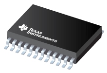
Datasheet Texas Instruments CDCE949-Q1
| Manufacturer | Texas Instruments |
| Series | CDCE949-Q1 |

Programmable 4-PLL VCXO Clock Synthesizer with 2.5V or 3.3V LVCMOS Outputs
Datasheets
CDCE949-Q1 Programmable 4-PLL VCXO Clock Synthesizer datasheet
PDF, 715 Kb, File published: Feb 3, 2010
Extract from the document
Prices
Status
| CDCE949QPWRQ1 | |
|---|---|
| Lifecycle Status | Active (Recommended for new designs) |
| Manufacture's Sample Availability | Yes |
Packaging
| CDCE949QPWRQ1 | |
|---|---|
| N | 1 |
| Pin | 24 |
| Package Type | PW |
| Industry STD Term | TSSOP |
| JEDEC Code | R-PDSO-G |
| Package QTY | 2000 |
| Carrier | LARGE T&R |
| Device Marking | CDCE949Q |
| Width (mm) | 4.4 |
| Length (mm) | 7.8 |
| Thickness (mm) | 1 |
| Pitch (mm) | .65 |
| Max Height (mm) | 1.2 |
| Mechanical Data | Download |
Parametrics
| Parameters / Models | CDCE949QPWRQ1 |
|---|---|
| Operating Temperature Range, C | -40 to 125 |
| Package Group | TSSOP |
| Package Size: mm2:W x L, PKG | 24TSSOP: 50 mm2: 6.4 x 7.8(TSSOP) |
Eco Plan
| CDCE949QPWRQ1 | |
|---|---|
| RoHS | Compliant |
Application Notes
- General I2C / EEPROM usage for the CDCE(L)9xx familyPDF, 40 Kb, File published: Jan 26, 2010
- Crystal or Crystal Oscillator Replacement with Silicon DevicesPDF, 894 Kb, File published: Jun 18, 2014
This application report is a general guide that outlines the advantages of using silicon-based timingdevices from Texas Instruments to generate system clocking solutions. This report covers theconventional way to derive system clocks using crystals and crystal oscillators, disadvantages of usingthese mechanical components, and details on replacing them with silicon-based timing devices from - VCXO Application Guideline for CDCE(L)9xx Family (Rev. A)PDF, 107 Kb, Revision: A, File published: Apr 23, 2012
- Usage of I2C for CDCE(L)949, CDCE(L)937, CDCE(L)925, CDCE(L)913PDF, 297 Kb, File published: Sep 23, 2009
This document presents a method to smoothly change frequency by IВІCв„ў protocol on Texas Instruments CDCE(L)949, CDCE(L)937, CDCE(L)925, CDCE(L)913 Clock Synthesizers, thus avoiding unnecessary intermediate frequencies. It also includes a code example to generate the IВІC protocol for the CDCE(L)9xx with the TMS320C645x. - Generating Low Phase-Noise Clocks for Audio Data Converters from Low FrequencyPDF, 860 Kb, File published: Mar 31, 2008
Generating a high-frequency system clock Fs (128fs to 768fs) from a low-frequency sampling clock fs (10 kHz to 200 kHz) is challenging, while attempting to maintain low phase jitter. A traditional phase-lock loop (PLL) can do the frequency translation, but the added phase jitter prevents the generated system clock signal from effectively driving high-performance audio data converters. This applica - Troubleshooting I2C Bus ProtocolPDF, 184 Kb, File published: Oct 19, 2009
When using the I2Cв„ў bus protocol, the designer must ensure that the hardware complies with the I2C standard. This application report describes the I2C protocol and provides guidelines on debugging a missing acknowledgment, selecting the pullup resistors, or meeting the maximum capacitance load of an I2C bus. A conflict occurs if devices sharing the I2C bus have the same slave address. This
Model Line
Series: CDCE949-Q1 (1)
Manufacturer's Classification
- Semiconductors> Staging> Unknown> Wired Communication / Networking / Storage Clocks
