Datasheet Texas Instruments CDCF5801A
| Manufacturer | Texas Instruments |
| Series | CDCF5801A |
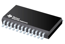
Low Jitter PLL Based Multiplier/Divider with programmable delay lines down to sub 10ps
Datasheets
Clock Multiplier With Delay Control and Phase Alignment datasheet
PDF, 603 Kb, File published: Mar 15, 2006
Extract from the document
Prices
Status
| CDCF5801ADBQ | CDCF5801ADBQG4 | CDCF5801ADBQR | CDCF5801ADBQRG4 | |
|---|---|---|---|---|
| Lifecycle Status | Active (Recommended for new designs) | Active (Recommended for new designs) | Active (Recommended for new designs) | Active (Recommended for new designs) |
| Manufacture's Sample Availability | Yes | Yes | Yes | Yes |
Packaging
| CDCF5801ADBQ | CDCF5801ADBQG4 | CDCF5801ADBQR | CDCF5801ADBQRG4 | |
|---|---|---|---|---|
| N | 1 | 2 | 3 | 4 |
| Pin | 24 | 24 | 24 | 24 |
| Package Type | DBQ | DBQ | DBQ | DBQ |
| Industry STD Term | SSOP | SSOP | SSOP | SSOP |
| JEDEC Code | R-PDSO-G | R-PDSO-G | R-PDSO-G | R-PDSO-G |
| Package QTY | 50 | 50 | 2500 | 2500 |
| Carrier | TUBE | TUBE | LARGE T&R | LARGE T&R |
| Device Marking | CDCF5801A | CDCF5801A | CDCF5801A | CDCF5801A |
| Width (mm) | 3.9 | 3.9 | 3.9 | 3.9 |
| Length (mm) | 8.65 | 8.65 | 8.65 | 8.65 |
| Thickness (mm) | 1.5 | 1.5 | 1.5 | 1.5 |
| Pitch (mm) | .64 | .64 | .64 | .64 |
| Max Height (mm) | 1.75 | 1.75 | 1.75 | 1.75 |
| Mechanical Data | Download | Download | Download | Download |
Parametrics
| Parameters / Models | CDCF5801ADBQ | CDCF5801ADBQG4 | CDCF5801ADBQR | CDCF5801ADBQRG4 |
|---|---|---|---|---|
| Input Level | HSTL,LVPECL,LVTTL | HSTL,LVPECL,LVTTL | HSTL,LVPECL,LVTTL | HSTL,LVPECL,LVTTL |
| Number of Outputs | 1 | 1 | 1 | 1 |
| Operating Temperature Range, C | -40 to 85 | -40 to 85 | -40 to 85 | -40 to 85 |
| Output Frequency(Max), MHz | 280 | 280 | 280 | 280 |
| Output Level | LVDS,LVPECL,LVTTL | LVDS,LVPECL,LVTTL | LVDS,LVPECL,LVTTL | LVDS,LVPECL,LVTTL |
| Package Group | SSOP | SSOP | SSOP | SSOP |
| Package Size: mm2:W x L, PKG | 24SSOP: 52 mm2: 6 x 8.65(SSOP) | 24SSOP: 52 mm2: 6 x 8.65(SSOP) | 24SSOP: 52 mm2: 6 x 8.65(SSOP) | 24SSOP: 52 mm2: 6 x 8.65(SSOP) |
| Programmability | Pin configuration | Pin configuration | Pin configuration | Pin configuration |
| Special Features | Spread Spectrum Clocking (SSC),3.3V Vcc/Vdd | Spread Spectrum Clocking (SSC),3.3V Vcc/Vdd | Spread Spectrum Clocking (SSC),3.3V Vcc/Vdd | Spread Spectrum Clocking (SSC),3.3V Vcc/Vdd |
| VCC Core, V | 3.3 | 3.3 | 3.3 | 3.3 |
| VCC Out, V | 3.3 | 3.3 | 3.3 | 3.3 |
Eco Plan
| CDCF5801ADBQ | CDCF5801ADBQG4 | CDCF5801ADBQR | CDCF5801ADBQRG4 | |
|---|---|---|---|---|
| RoHS | Compliant | Compliant | Compliant | Compliant |
Application Notes
- A General Guideline: How to Use the CDCF5801A for Phase Alignment/Adjustment (Rev. B)PDF, 129 Kb, Revision: B, File published: Oct 21, 2005
Unlike regular PLLs, the CDCF5801 has an extra phase aligner. Using this extra phase aligner, the CDCF5801 can align two different clock phases, even with differentfrequencies. Examples of where phase alignment may be useful include:В· Applications where two clock buffers' outputs need to be alignedВ· Applications that require data synchronization with SERDESВ· Applications that require stati - Using Configurable Active Delay Elements in CDCF5801A Feedback LoopPDF, 43 Kb, File published: Sep 15, 2004
Using Configurable Active Delay Elements in CDCF5801 Feedback Loop
Model Line
Series: CDCF5801A (4)
Manufacturer's Classification
- Semiconductors> Clock and Timing> Clock Generators> General Purpose
