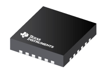
CDCP1803
www.ti.com SCAS727F – NOVEMBER 2003 – REVISED DECEMBER 2013 1:3 LVPECL CLOCK BUFFER
WITH PROGRAMMABLE DIVIDER
Check for Samples: CDCP1803 FEATURES 1 S1 VDD0 Y0 Y0 VDD0 24 23 22 21 20 19
18 VDDPECL 2 17 VDD1 IN 3 16 Y1 IN 4 15 Y1 VDDPECL 5 14 VDD1 VBB 6 (1) VSS(1) 9 13
10 11 12 S0 VSS NC 8 VDD2 7 Y2 1 Y2 EN VDD2 RGE PACKAGE
(TOP VIEW) S2 Distributes One Differential Clock Input to
Three LVPECL Differential Clock Outputs
Programmable Output Divider for Two LVPECL
Outputs
Low-Output Skew 15 ps (Typical)
VCC Range 3 V–3.6 V
Signaling Rate Up to 800-MHz LVPECL
Differential Input Stage for Wide CommonMode Range
Provides VBB Bias Voltage Output for SingleEnded Input Signals
Receiver Input Threshold В±75 mV
24-Terminal QFN Package (4 mm Г— 4 mm)
Accepts Any Differential Signaling:
LVDS, HSTL, CML, VML, SSTL-2, and
Single-Ended: LVTTL/LVCMOS VSS Thermal pad must be connected to VSS. P0024-02 DESCRIPTION S2 VDD0 Y0 Y0 VDD0 S1 23 22 21 20 19 EN 1 18 S0 VDDPECL 2 17 VDD1 IN 3 16 Y1 IN 4 15 Y1 VDDPECL 5 14 VDD1 VBB 6 13 VSS (1) 7 8 9 10 11 12 VDD2 Y2 Y2 VDD2 NC VSS(1) VSS The CDCP1803 has three control terminals, S0, S1,
and S2, to select different output mode settings; see
Table 1 for details. The CDCP1803 is characterized
for operation from –40В°C to 85В°C. For use in singleended driver applications, the CDCP1803 also …

