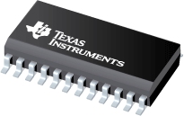
Datasheet Texas Instruments SN74BCT8374A
| Manufacturer | Texas Instruments |
| Series | SN74BCT8374A |

Scan Test Device With Octal D-Type Edge-Triggered Flip-Flops
Datasheets
Scan Test Devices With Octal D-Type Edge-Triggered Flip-Flops datasheet
PDF, 435 Kb, Revision: E, File published: Jul 1, 1996
Extract from the document
Prices
Status
| SN74BCT8374ADW | |
|---|---|
| Lifecycle Status | Active (Recommended for new designs) |
| Manufacture's Sample Availability | No |
Packaging
| SN74BCT8374ADW | |
|---|---|
| N | 1 |
| Pin | 24 |
| Package Type | DW |
| Industry STD Term | SOIC |
| JEDEC Code | R-PDSO-G |
| Package QTY | 25 |
| Carrier | TUBE |
| Device Marking | BCT8374A |
| Width (mm) | 7.5 |
| Length (mm) | 15.4 |
| Thickness (mm) | 2.35 |
| Pitch (mm) | 1.27 |
| Max Height (mm) | 2.65 |
| Mechanical Data | Download |
Parametrics
| Parameters / Models | SN74BCT8374ADW |
|---|---|
| Bits | 8 |
| F @ Nom Voltage(Max), Mhz | 70 |
| ICC @ Nom Voltage(Max), mA | 52 |
| Operating Temperature Range, C | 0 to 70 |
| Output Drive (IOL/IOH)(Max), mA | 64/-15 |
| Package Group | SOIC |
| Package Size: mm2:W x L, PKG | 24SOIC: 160 mm2: 10.3 x 15.5(SOIC) |
| Rating | Catalog |
| Technology Family | BCT |
| VCC(Max), V | 5.5 |
| VCC(Min), V | 4.5 |
| Voltage(Nom), V | 5 |
| tpd @ Nom Voltage(Max), ns | 10 |
Eco Plan
| SN74BCT8374ADW | |
|---|---|
| RoHS | Compliant |
Application Notes
- Programming CPLDs Via the 'LVT8986 LASPPDF, 819 Kb, File published: Nov 1, 2005
This application report summarizes key information required for understanding the 'LVT8986 linking addressable scan ports (LASPs) multidrop addressable IEEE Std 1149.1 (JTAG) test access port (TAP) transceiver. This report includes information about the 'LVT8986 secondary TAPs, bypass and linking shadow protocol, scan-path description languages, serial vector format files, and an example of how to
Model Line
Series: SN74BCT8374A (1)
Manufacturer's Classification
- Semiconductors> Logic> Specialty Logic> Boundary Scan (JTAG) Logic
