Datasheet Texas Instruments TMS320DM648
| Manufacturer | Texas Instruments |
| Series | TMS320DM648 |
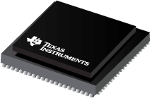
Digital Media Processor
Datasheets
TMS320DM647/TMS320DM648 Digital Media Processors datasheet
PDF, 1.4 Mb, Revision: H, File published: Apr 10, 2012
Extract from the document
Prices
Status
| TMS320DM648CUT1 | TMS320DM648CUT7 | TMS320DM648CUT9 | TMS320DM648CUTA6 | TMS320DM648CUTA8 | TMS320DM648CUTD1 | TMS320DM648CUTD7 | TMS320DM648CUTD9 | TMS320DM648ZUT1 | TMS320DM648ZUT7 | TMS320DM648ZUT9 | TMS320DM648ZUT9HK | TMS320DM648ZUTA6 | TMS320DM648ZUTA8 | TMS320DM648ZUTD1 | TMS320DM648ZUTD7 | TMS320DM648ZUTD9 | TNETV2685FIBZUT11 | TNETV2685FIBZUT5 | TNETV2685FIBZUT7 | TNETV2685FIBZUT9 | TNETV2685FIBZUTA11 | TNETV2685FIBZUTA5 | TNETV2685FIBZUTA7 | TNETV2685FIBZUTA9 | TNETV2685FIDZUT11 | TNETV2685FIDZUT5 | TNETV2685FIDZUT7 | TNETV2685FIDZUT9 | TNETV2685FIDZUTA11 | TNETV2685FIDZUTA5 | TNETV2685FIDZUTA7 | TNETV2685FIDZUTA9 | TNETV2685VIDZUT11 | TNETV2685VIDZUT5 | TNETV2685VIDZUT7 | TNETV2685VIDZUT9 | TNETV2685VIDZUTA11 | TNETV2685VIDZUTA5 | TNETV2685VIDZUTA7 | TNETV2685VIDZUTA9 | TNETV2685ZUT11 | TNETV2685ZUT5 | TNETV2685ZUT7 | TNETV2685ZUT9 | TNETV2685ZUTA11 | TNETV2685ZUTA5 | TNETV2685ZUTA7 | TNETV2685ZUTA9 | VCBUSAM648T9 | |
|---|---|---|---|---|---|---|---|---|---|---|---|---|---|---|---|---|---|---|---|---|---|---|---|---|---|---|---|---|---|---|---|---|---|---|---|---|---|---|---|---|---|---|---|---|---|---|---|---|---|---|
| Lifecycle Status | Obsolete (Manufacturer has discontinued the production of the device) | NRND (Not recommended for new designs) | Active (Recommended for new designs) | NRND (Not recommended for new designs) | NRND (Not recommended for new designs) | Obsolete (Manufacturer has discontinued the production of the device) | NRND (Not recommended for new designs) | NRND (Not recommended for new designs) | Obsolete (Manufacturer has discontinued the production of the device) | NRND (Not recommended for new designs) | NRND (Not recommended for new designs) | NRND (Not recommended for new designs) | NRND (Not recommended for new designs) | NRND (Not recommended for new designs) | Obsolete (Manufacturer has discontinued the production of the device) | NRND (Not recommended for new designs) | NRND (Not recommended for new designs) | Obsolete (Manufacturer has discontinued the production of the device) | NRND (Not recommended for new designs) | NRND (Not recommended for new designs) | NRND (Not recommended for new designs) | Obsolete (Manufacturer has discontinued the production of the device) | NRND (Not recommended for new designs) | NRND (Not recommended for new designs) | NRND (Not recommended for new designs) | Obsolete (Manufacturer has discontinued the production of the device) | NRND (Not recommended for new designs) | NRND (Not recommended for new designs) | NRND (Not recommended for new designs) | Obsolete (Manufacturer has discontinued the production of the device) | NRND (Not recommended for new designs) | NRND (Not recommended for new designs) | NRND (Not recommended for new designs) | Obsolete (Manufacturer has discontinued the production of the device) | NRND (Not recommended for new designs) | NRND (Not recommended for new designs) | NRND (Not recommended for new designs) | Obsolete (Manufacturer has discontinued the production of the device) | NRND (Not recommended for new designs) | NRND (Not recommended for new designs) | NRND (Not recommended for new designs) | Obsolete (Manufacturer has discontinued the production of the device) | NRND (Not recommended for new designs) | NRND (Not recommended for new designs) | NRND (Not recommended for new designs) | Obsolete (Manufacturer has discontinued the production of the device) | NRND (Not recommended for new designs) | NRND (Not recommended for new designs) | NRND (Not recommended for new designs) | NRND (Not recommended for new designs) |
| Manufacture's Sample Availability | No | No | No | No | No | No | No | No | No | No | No | No | No | No | No | No | No | No | No | No | No | No | No | No | No | No | No | No | No | No | No | No | No | No | No | No | No | No | No | No | No | No | No | No | No | No | No | No | No | No |
Packaging
| TMS320DM648CUT1 | TMS320DM648CUT7 | TMS320DM648CUT9 | TMS320DM648CUTA6 | TMS320DM648CUTA8 | TMS320DM648CUTD1 | TMS320DM648CUTD7 | TMS320DM648CUTD9 | TMS320DM648ZUT1 | TMS320DM648ZUT7 | TMS320DM648ZUT9 | TMS320DM648ZUT9HK | TMS320DM648ZUTA6 | TMS320DM648ZUTA8 | TMS320DM648ZUTD1 | TMS320DM648ZUTD7 | TMS320DM648ZUTD9 | TNETV2685FIBZUT11 | TNETV2685FIBZUT5 | TNETV2685FIBZUT7 | TNETV2685FIBZUT9 | TNETV2685FIBZUTA11 | TNETV2685FIBZUTA5 | TNETV2685FIBZUTA7 | TNETV2685FIBZUTA9 | TNETV2685FIDZUT11 | TNETV2685FIDZUT5 | TNETV2685FIDZUT7 | TNETV2685FIDZUT9 | TNETV2685FIDZUTA11 | TNETV2685FIDZUTA5 | TNETV2685FIDZUTA7 | TNETV2685FIDZUTA9 | TNETV2685VIDZUT11 | TNETV2685VIDZUT5 | TNETV2685VIDZUT7 | TNETV2685VIDZUT9 | TNETV2685VIDZUTA11 | TNETV2685VIDZUTA5 | TNETV2685VIDZUTA7 | TNETV2685VIDZUTA9 | TNETV2685ZUT11 | TNETV2685ZUT5 | TNETV2685ZUT7 | TNETV2685ZUT9 | TNETV2685ZUTA11 | TNETV2685ZUTA5 | TNETV2685ZUTA7 | TNETV2685ZUTA9 | VCBUSAM648T9 | |
|---|---|---|---|---|---|---|---|---|---|---|---|---|---|---|---|---|---|---|---|---|---|---|---|---|---|---|---|---|---|---|---|---|---|---|---|---|---|---|---|---|---|---|---|---|---|---|---|---|---|---|
| N | 1 | 2 | 3 | 4 | 5 | 6 | 7 | 8 | 9 | 10 | 11 | 12 | 13 | 14 | 15 | 16 | 17 | 18 | 19 | 20 | 21 | 22 | 23 | 24 | 25 | 26 | 27 | 28 | 29 | 30 | 31 | 32 | 33 | 34 | 35 | 36 | 37 | 38 | 39 | 40 | 41 | 42 | 43 | 44 | 45 | 46 | 47 | 48 | 49 | 50 |
| Pin | 529 | 529 | 529 | 529 | 529 | 529 | 529 | 529 | 529 | 529 | 529 | 529 | 529 | 529 | 529 | 529 | 529 | 529 | 529 | 529 | 529 | 529 | 529 | 529 | 529 | 529 | 529 | 529 | 529 | 529 | 529 | 529 | 529 | 529 | 529 | 529 | 529 | 529 | 529 | 529 | 529 | 529 | 529 | 529 | 529 | 529 | 529 | 529 | 529 | 529 |
| Package Type | CUT | CUT | CUT | CUT | CUT | CUT | CUT | CUT | ZUT | ZUT | ZUT | ZUT | ZUT | ZUT | ZUT | ZUT | ZUT | ZUT | ZUT | ZUT | ZUT | ZUT | ZUT | ZUT | ZUT | ZUT | ZUT | ZUT | ZUT | ZUT | ZUT | ZUT | ZUT | ZUT | ZUT | ZUT | ZUT | ZUT | ZUT | ZUT | ZUT | ZUT | ZUT | ZUT | ZUT | ZUT | ZUT | ZUT | ZUT | ZUT |
| Device Marking | TMS320DM648CUT | 720MHZ | TMS320DM648CUT | @2007 TI | TMS320DM648CUT | @2007 TI | @2007 TI | D900MHZ | @2007 TI | @2007 TI | TMS320DM648ZUT | TMS320DM648ZUT | A600MHZ | A800MHZ | D1.1GHZ | TMS320DM648ZUT | D900MHZ | TMS320DM648ZUT | TMS320DM648ZUT | TMS320DM648ZUT | @2007 TI | TMS320DM648ZUT | TMS320DM648ZUT | @2007 TI | @2007 TI | TMS320DM648ZUT | @2007 TI | TMS320DM648ZUT | TMS320DM648ZUT | TMS320DM648ZUT | D720MHZ | @2007 TI | @2007 TI | TMS320DM648ZUT | 720MHZ | TMS320DM648ZUT | TMS320DM648ZUT | @2007 TI | D720MHZ | D720MHZ | D900MHZ | @2007 TI | @2007 TI | @2007 TI | @2007 TI | D1.1GHZ | @2007 TI | @2007 TI | @2007 TI | @2007 TI |
| Width (mm) | 19 | 19 | 19 | 19 | 19 | 19 | 19 | 19 | 19 | 19 | 19 | 19 | 19 | 19 | 19 | 19 | 19 | 19 | 19 | 19 | 19 | 19 | 19 | 19 | 19 | 19 | 19 | 19 | 19 | 19 | 19 | 19 | 19 | 19 | 19 | 19 | 19 | 19 | 19 | 19 | 19 | 19 | 19 | 19 | 19 | 19 | 19 | 19 | 19 | 19 |
| Length (mm) | 19 | 19 | 19 | 19 | 19 | 19 | 19 | 19 | 19 | 19 | 19 | 19 | 19 | 19 | 19 | 19 | 19 | 19 | 19 | 19 | 19 | 19 | 19 | 19 | 19 | 19 | 19 | 19 | 19 | 19 | 19 | 19 | 19 | 19 | 19 | 19 | 19 | 19 | 19 | 19 | 19 | 19 | 19 | 19 | 19 | 19 | 19 | 19 | 19 | 19 |
| Thickness (mm) | 2.65 | 2.65 | 2.65 | 2.65 | 2.65 | 2.65 | 2.65 | 2.65 | 2.65 | 2.65 | 2.65 | 2.65 | 2.65 | 2.65 | 2.65 | 2.65 | 2.65 | 2.65 | 2.65 | 2.65 | 2.65 | 2.65 | 2.65 | 2.65 | 2.65 | 2.65 | 2.65 | 2.65 | 2.65 | 2.65 | 2.65 | 2.65 | 2.65 | 2.65 | 2.65 | 2.65 | 2.65 | 2.65 | 2.65 | 2.65 | 2.65 | 2.65 | 2.65 | 2.65 | 2.65 | 2.65 | 2.65 | 2.65 | 2.65 | 2.65 |
| Mechanical Data | Download | Download | Download | Download | Download | Download | Download | Download | Download | Download | Download | Download | Download | Download | Download | Download | Download | Download | Download | Download | Download | Download | Download | Download | Download | Download | Download | Download | Download | Download | Download | Download | Download | Download | Download | Download | Download | Download | Download | Download | Download | Download | Download | Download | Download | Download | Download | Download | Download | Download |
| Package QTY | 84 | 84 | 84 | 84 | 84 | 84 | 84 | 84 | 84 | 84 | 84 | 84 | 84 | 84 | 84 | 84 | 84 | 84 | 84 | 84 | 84 | 84 | 84 | 84 | 84 | 84 | 84 | 84 | 84 | 84 | 84 | 84 | 84 | 84 | 84 | 84 | ||||||||||||||
| Carrier | JEDEC TRAY (5+1) | JEDEC TRAY (5+1) | JEDEC TRAY (5+1) | JEDEC TRAY (5+1) | JEDEC TRAY (5+1) | JEDEC TRAY (5+1) | JEDEC TRAY (5+1) | JEDEC TRAY (5+1) | JEDEC TRAY (5+1) | JEDEC TRAY (5+1) | JEDEC TRAY (5+1) | JEDEC TRAY (5+1) | JEDEC TRAY (5+1) | JEDEC TRAY (5+1) | JEDEC TRAY (5+1) | JEDEC TRAY (5+1) | JEDEC TRAY (5+1) | JEDEC TRAY (5+1) | JEDEC TRAY (5+1) | JEDEC TRAY (5+1) | JEDEC TRAY (5+1) | JEDEC TRAY (5+1) | JEDEC TRAY (5+1) | JEDEC TRAY (5+1) | JEDEC TRAY (5+1) | JEDEC TRAY (5+1) | JEDEC TRAY (5+1) | JEDEC TRAY (5+1) | JEDEC TRAY (5+1) | JEDEC TRAY (5+1) | JEDEC TRAY (5+1) | JEDEC TRAY (5+1) | JEDEC TRAY (5+1) | JEDEC TRAY (5+1) | JEDEC TRAY (5+1) | JEDEC TRAY (5+1) | JEDEC TRAY (5+1) | JEDEC TRAY (5+1) | JEDEC TRAY (5+1) | JEDEC TRAY (5+1) | ||||||||||
| Industry STD Term | FCBGA | FCBGA | FCBGA | FCBGA | FCBGA | FCBGA | FCBGA | FCBGA | FCBGA | FCBGA | FCBGA | FCBGA | FCBGA | FCBGA | FCBGA | FCBGA | FCBGA | FCBGA | FCBGA | FCBGA | FCBGA | FCBGA | FCBGA | FCBGA | FCBGA | FCBGA | FCBGA | FCBGA | FCBGA | FCBGA | FCBGA | FCBGA | FCBGA | FCBGA | FCBGA | FCBGA | FCBGA | FCBGA | FCBGA | FCBGA | FCBGA | FCBGA | ||||||||
| JEDEC Code | S-PBGA-N | S-PBGA-N | S-PBGA-N | S-PBGA-N | S-PBGA-N | S-PBGA-N | S-PBGA-N | S-PBGA-N | S-PBGA-N | S-PBGA-N | S-PBGA-N | S-PBGA-N | S-PBGA-N | S-PBGA-N | S-PBGA-N | S-PBGA-N | S-PBGA-N | S-PBGA-N | S-PBGA-N | S-PBGA-N | S-PBGA-N | S-PBGA-N | S-PBGA-N | S-PBGA-N | S-PBGA-N | S-PBGA-N | S-PBGA-N | S-PBGA-N | S-PBGA-N | S-PBGA-N | S-PBGA-N | S-PBGA-N | S-PBGA-N | S-PBGA-N | S-PBGA-N | S-PBGA-N | S-PBGA-N | S-PBGA-N | S-PBGA-N | S-PBGA-N | S-PBGA-N | S-PBGA-N | ||||||||
| Pitch (mm) | .8 | .8 | .8 | .8 | .8 | .8 | .8 | .8 | .8 | .8 | .8 | .8 | .8 | .8 | .8 | .8 | .8 | .8 | .8 | .8 | .8 | .8 | .8 | .8 | .8 | .8 | .8 | .8 | .8 | .8 | .8 | .8 | .8 | .8 | .8 | .8 | .8 | .8 | .8 | .8 | .8 | .8 | ||||||||
| Max Height (mm) | 3.3 | 3.3 | 3.3 | 3.3 | 3.3 | 3.3 | 3.3 | 3.3 | 3.3 | 3.3 | 3.3 | 3.3 | 3.3 | 3.3 | 3.3 | 3.3 | 3.3 | 3.3 | 3.3 | 3.3 | 3.3 | 3.3 | 3.3 | 3.3 | 3.3 | 3.3 | 3.3 | 3.3 | 3.3 | 3.3 | 3.3 | 3.3 | 3.3 | 3.3 | 3.3 | 3.3 | 3.3 | 3.3 | 3.3 | 3.3 | 3.3 | 3.3 |
Parametrics
| Parameters / Models | TMS320DM648CUT1 | TMS320DM648CUT7 | TMS320DM648CUT9 | TMS320DM648CUTA6 | TMS320DM648CUTA8 | TMS320DM648CUTD1 | TMS320DM648CUTD7 | TMS320DM648CUTD9 | TMS320DM648ZUT1 | TMS320DM648ZUT7 | TMS320DM648ZUT9 | TMS320DM648ZUT9HK | TMS320DM648ZUTA6 | TMS320DM648ZUTA8 | TMS320DM648ZUTD1 | TMS320DM648ZUTD7 | TMS320DM648ZUTD9 | TNETV2685FIBZUT11 | TNETV2685FIBZUT5 | TNETV2685FIBZUT7 | TNETV2685FIBZUT9 | TNETV2685FIBZUTA11 | TNETV2685FIBZUTA5 | TNETV2685FIBZUTA7 | TNETV2685FIBZUTA9 | TNETV2685FIDZUT11 | TNETV2685FIDZUT5 | TNETV2685FIDZUT7 | TNETV2685FIDZUT9 | TNETV2685FIDZUTA11 | TNETV2685FIDZUTA5 | TNETV2685FIDZUTA7 | TNETV2685FIDZUTA9 | TNETV2685VIDZUT11 | TNETV2685VIDZUT5 | TNETV2685VIDZUT7 | TNETV2685VIDZUT9 | TNETV2685VIDZUTA11 | TNETV2685VIDZUTA5 | TNETV2685VIDZUTA7 | TNETV2685VIDZUTA9 | TNETV2685ZUT11 | TNETV2685ZUT5 | TNETV2685ZUT7 | TNETV2685ZUT9 | TNETV2685ZUTA11 | TNETV2685ZUTA5 | TNETV2685ZUTA7 | TNETV2685ZUTA9 | VCBUSAM648T9 |
|---|---|---|---|---|---|---|---|---|---|---|---|---|---|---|---|---|---|---|---|---|---|---|---|---|---|---|---|---|---|---|---|---|---|---|---|---|---|---|---|---|---|---|---|---|---|---|---|---|---|---|
| Applications | Automotive Industrial Video and Imaging | Automotive,Industrial,Video and Imaging | Automotive,Industrial,Video and Imaging | Automotive,Industrial,Video and Imaging | Automotive,Industrial,Video and Imaging | Automotive Industrial Video and Imaging | Automotive,Industrial,Video and Imaging | Automotive,Industrial,Video and Imaging | Automotive,Industrial,Video and Imaging | Automotive,Industrial,Video and Imaging | Automotive,Industrial,Video and Imaging | Automotive,Industrial,Video and Imaging | Automotive Industrial Video and Imaging | Automotive,Industrial,Video and Imaging | Automotive Industrial Video and Imaging | Automotive,Industrial,Video and Imaging | Automotive,Industrial,Video and Imaging | Automotive,Industrial,Video and Imaging | Automotive,Industrial,Video and Imaging | Automotive,Industrial,Video and Imaging | Automotive,Industrial,Video and Imaging | Automotive Industrial Video and Imaging | Automotive,Industrial,Video and Imaging | Automotive,Industrial,Video and Imaging | Automotive,Industrial,Video and Imaging | Automotive,Industrial,Video and Imaging | Automotive,Industrial,Video and Imaging | Automotive,Industrial,Video and Imaging | Automotive,Industrial,Video and Imaging | Automotive Industrial Video and Imaging | Automotive,Industrial,Video and Imaging | Automotive,Industrial,Video and Imaging | Automotive,Industrial,Video and Imaging | Automotive,Industrial,Video and Imaging | Automotive,Industrial,Video and Imaging | Automotive,Industrial,Video and Imaging | Automotive,Industrial,Video and Imaging | Automotive Industrial Video and Imaging | Automotive,Industrial,Video and Imaging | Automotive,Industrial,Video and Imaging | Automotive,Industrial,Video and Imaging | Automotive,Industrial,Video and Imaging | Automotive,Industrial,Video and Imaging | Automotive,Industrial,Video and Imaging | Automotive,Industrial,Video and Imaging | Automotive Industrial Video and Imaging | Automotive,Industrial,Video and Imaging | Automotive,Industrial,Video and Imaging | Automotive,Industrial,Video and Imaging | Automotive,Industrial,Video and Imaging |
| Approx. Price (US$) | 59.10 | 1ku | 59.10 | 1ku | 59.10 | 1ku | 59.10 | 1ku | 59.10 | 1ku | 59.10 | 1ku | 59.10 | 1ku | 59.10 | 1ku | ||||||||||||||||||||||||||||||||||||||||||
| DRAM | DDR2 | DDR2 | DDR2 | DDR2 | DDR2 | DDR2 | DDR2 | DDR2 | DDR2 | DDR2 | DDR2 | DDR2 | DDR2 | DDR2 | DDR2 | DDR2 | DDR2 | DDR2 | DDR2 | DDR2 | DDR2 | DDR2 | DDR2 | DDR2 | DDR2 | DDR2 | DDR2 | DDR2 | DDR2 | DDR2 | DDR2 | DDR2 | DDR2 | DDR2 | DDR2 | DDR2 | DDR2 | DDR2 | DDR2 | DDR2 | DDR2 | DDR2 | DDR2 | DDR2 | DDR2 | DDR2 | DDR2 | DDR2 | DDR2 | DDR2 |
| DSP | 1 C64x | 1 C64x | 1 C64x | 1 C64x | 1 C64x | 1 C64x | 1 C64x | 1 C64x | 1 C64x | 1 C64x | 1 C64x | 1 C64x | 1 C64x | 1 C64x | 1 C64x | 1 C64x | 1 C64x | 1 C64x | 1 C64x | 1 C64x | 1 C64x | 1 C64x | 1 C64x | 1 C64x | 1 C64x | 1 C64x | 1 C64x | 1 C64x | 1 C64x | 1 C64x | 1 C64x | 1 C64x | 1 C64x | 1 C64x | 1 C64x | 1 C64x | 1 C64x | 1 C64x | 1 C64x | 1 C64x | 1 C64x | 1 C64x | 1 C64x | 1 C64x | 1 C64x | 1 C64x | 1 C64x | 1 C64x | 1 C64x | 1 C64x |
| DSP MHz, Max. | 720,800,900,1100 | 720,800,900,1100 | 720,800,900,1100 | 720,800,900,1100 | 720,800,900,1100 | 720,800,900,1100 | 720,800,900,1100 | 720,800,900,1100 | 720,800,900,1100 | 720,800,900,1100 | 720,800,900,1100 | 720,800,900,1100 | 720,800,900,1100 | 720,800,900,1100 | 720,800,900,1100 | 720,800,900,1100 | 720,800,900,1100 | 720,800,900,1100 | 720,800,900,1100 | 720,800,900,1100 | 720,800,900,1100 | 720,800,900,1100 | 720,800,900,1100 | 720,800,900,1100 | 720,800,900,1100 | 720,800,900,1100 | 720,800,900,1100 | 720,800,900,1100 | 720,800,900,1100 | 720,800,900,1100 | 720,800,900,1100 | 720,800,900,1100 | 720,800,900,1100 | 720,800,900,1100 | 720,800,900,1100 | 720,800,900,1100 | 720,800,900,1100 | 720,800,900,1100 | 720,800,900,1100 | 720,800,900,1100 | 720,800,900,1100 | 720,800,900,1100 | ||||||||
| DSP MHz (Max.) | 720 800 900 1100 | 720 800 900 1100 | 720 800 900 1100 | 720 800 900 1100 | 720 800 900 1100 | 720 800 900 1100 | 720 800 900 1100 | 720 800 900 1100 | ||||||||||||||||||||||||||||||||||||||||||
| I2C | 1 | 1 | 1 | 1 | 1 | 1 | 1 | 1 | 1 | 1 | 1 | 1 | 1 | 1 | 1 | 1 | 1 | 1 | 1 | 1 | 1 | 1 | 1 | 1 | 1 | 1 | 1 | 1 | 1 | 1 | 1 | 1 | 1 | 1 | 1 | 1 | 1 | 1 | 1 | 1 | 1 | 1 | 1 | 1 | 1 | 1 | 1 | 1 | 1 | 1 |
| On-Chip L2 Cache | 512 KB(DSP) | 512 KB(DSP) | 512 KB(DSP) | 512 KB(DSP) | 512 KB(DSP) | 512 KB(DSP) | 512 KB(DSP) | 512 KB(DSP) | 512 KB(DSP) | 512 KB(DSP) | 512 KB(DSP) | 512 KB(DSP) | 512 KB(DSP) | 512 KB(DSP) | 512 KB(DSP) | 512 KB(DSP) | 512 KB(DSP) | 512 KB(DSP) | 512 KB(DSP) | 512 KB(DSP) | 512 KB(DSP) | 512 KB(DSP) | 512 KB(DSP) | 512 KB(DSP) | 512 KB(DSP) | 512 KB(DSP) | 512 KB(DSP) | 512 KB(DSP) | 512 KB(DSP) | 512 KB(DSP) | 512 KB(DSP) | 512 KB(DSP) | 512 KB(DSP) | 512 KB(DSP) | 512 KB(DSP) | 512 KB(DSP) | 512 KB(DSP) | 512 KB(DSP) | 512 KB(DSP) | 512 KB(DSP) | 512 KB(DSP) | 512 KB(DSP) | 512 KB(DSP) | 512 KB(DSP) | 512 KB(DSP) | 512 KB(DSP) | 512 KB(DSP) | 512 KB(DSP) | 512 KB(DSP) | 512 KB(DSP) |
| Operating Systems | DSP/BIOS VLX | DSP/BIOS,VLX | DSP/BIOS,VLX | DSP/BIOS,VLX | DSP/BIOS,VLX | DSP/BIOS VLX | DSP/BIOS,VLX | DSP/BIOS,VLX | DSP/BIOS,VLX | DSP/BIOS,VLX | DSP/BIOS,VLX | DSP/BIOS,VLX | DSP/BIOS VLX | DSP/BIOS,VLX | DSP/BIOS VLX | DSP/BIOS,VLX | DSP/BIOS,VLX | DSP/BIOS,VLX | DSP/BIOS,VLX | DSP/BIOS,VLX | DSP/BIOS,VLX | DSP/BIOS VLX | DSP/BIOS,VLX | DSP/BIOS,VLX | DSP/BIOS,VLX | DSP/BIOS,VLX | DSP/BIOS,VLX | DSP/BIOS,VLX | DSP/BIOS,VLX | DSP/BIOS VLX | DSP/BIOS,VLX | DSP/BIOS,VLX | DSP/BIOS,VLX | DSP/BIOS,VLX | DSP/BIOS,VLX | DSP/BIOS,VLX | DSP/BIOS,VLX | DSP/BIOS VLX | DSP/BIOS,VLX | DSP/BIOS,VLX | DSP/BIOS,VLX | DSP/BIOS,VLX | DSP/BIOS,VLX | DSP/BIOS,VLX | DSP/BIOS,VLX | DSP/BIOS VLX | DSP/BIOS,VLX | DSP/BIOS,VLX | DSP/BIOS,VLX | DSP/BIOS,VLX |
| Operating Temperature Range, C | 0 to 90 | 0 to 90 | 0 to 90 | 0 to 90 | 0 to 90 | 0 to 90 | 0 to 90 | 0 to 90 | 0 to 90 | 0 to 90 | 0 to 90 | 0 to 90 | 0 to 90 | 0 to 90 | 0 to 90 | 0 to 90 | 0 to 90 | 0 to 90 | 0 to 90 | 0 to 90 | 0 to 90 | 0 to 90 | 0 to 90 | 0 to 90 | 0 to 90 | 0 to 90 | 0 to 90 | 0 to 90 | 0 to 90 | 0 to 90 | 0 to 90 | 0 to 90 | 0 to 90 | 0 to 90 | 0 to 90 | 0 to 90 | 0 to 90 | 0 to 90 | 0 to 90 | 0 to 90 | 0 to 90 | 0 to 90 | ||||||||
| Operating Temperature Range(C) | -40 to 90 0 to 90 | -40 to 90 0 to 90 | -40 to 90 0 to 90 | -40 to 90 0 to 90 | -40 to 90 0 to 90 | -40 to 90 0 to 90 | -40 to 90 0 to 90 | -40 to 90 0 to 90 | ||||||||||||||||||||||||||||||||||||||||||
| PCI/PCIe | 1 32-Bit [66 MHz] | 1 32-Bit [66 MHz] | 1 32-Bit [66 MHz] | 1 32-Bit [66 MHz] | 1 32-Bit [66 MHz] | 1 32-Bit [66 MHz] | 1 32-Bit [66 MHz] | 1 32-Bit [66 MHz] | 1 32-Bit [66 MHz] | 1 32-Bit [66 MHz] | 1 32-Bit [66 MHz] | 1 32-Bit [66 MHz] | 1 32-Bit [66 MHz] | 1 32-Bit [66 MHz] | 1 32-Bit [66 MHz] | 1 32-Bit [66 MHz] | 1 32-Bit [66 MHz] | 1 32-Bit [66 MHz] | 1 32-Bit [66 MHz] | 1 32-Bit [66 MHz] | 1 32-Bit [66 MHz] | 1 32-Bit [66 MHz] | 1 32-Bit [66 MHz] | 1 32-Bit [66 MHz] | 1 32-Bit [66 MHz] | 1 32-Bit [66 MHz] | 1 32-Bit [66 MHz] | 1 32-Bit [66 MHz] | 1 32-Bit [66 MHz] | 1 32-Bit [66 MHz] | 1 32-Bit [66 MHz] | 1 32-Bit [66 MHz] | 1 32-Bit [66 MHz] | 1 32-Bit [66 MHz] | 1 32-Bit [66 MHz] | 1 32-Bit [66 MHz] | 1 32-Bit [66 MHz] | 1 32-Bit [66 MHz] | 1 32-Bit [66 MHz] | 1 32-Bit [66 MHz] | 1 32-Bit [66 MHz] | 1 32-Bit [66 MHz] | 1 32-Bit [66 MHz] | 1 32-Bit [66 MHz] | 1 32-Bit [66 MHz] | 1 32-Bit [66 MHz] | 1 32-Bit [66 MHz] | 1 32-Bit [66 MHz] | 1 32-Bit [66 MHz] | 1 32-Bit [66 MHz] |
| Pin/Package | 529FCBGA | 529FCBGA | 529FCBGA | 529FCBGA | 529FCBGA | 529FCBGA | 529FCBGA | 529FCBGA | 529FCBGA | 529FCBGA | 529FCBGA | 529FCBGA | 529FCBGA | 529FCBGA | 529FCBGA | 529FCBGA | 529FCBGA | 529FCBGA | 529FCBGA | 529FCBGA | 529FCBGA | 529FCBGA | 529FCBGA | 529FCBGA | 529FCBGA | 529FCBGA | 529FCBGA | 529FCBGA | 529FCBGA | 529FCBGA | 529FCBGA | 529FCBGA | 529FCBGA | 529FCBGA | 529FCBGA | 529FCBGA | 529FCBGA | 529FCBGA | 529FCBGA | 529FCBGA | 529FCBGA | 529FCBGA | 529FCBGA | 529FCBGA | 529FCBGA | 529FCBGA | 529FCBGA | 529FCBGA | 529FCBGA | 529FCBGA |
| Rating | Catalog | Catalog | Catalog | Catalog | Catalog | Catalog | Catalog | Catalog | Catalog | Catalog | Catalog | Catalog | Catalog | Catalog | Catalog | Catalog | Catalog | Catalog | Catalog | Catalog | Catalog | Catalog | Catalog | Catalog | Catalog | Catalog | Catalog | Catalog | Catalog | Catalog | Catalog | Catalog | Catalog | Catalog | Catalog | Catalog | Catalog | Catalog | Catalog | Catalog | Catalog | Catalog | Catalog | Catalog | Catalog | Catalog | Catalog | Catalog | Catalog | Catalog |
| Video Acceleration | 1 VICP | 1 VICP | 1 VICP | 1 VICP | 1 VICP | 1 VICP | 1 VICP | 1 VICP | 1 VICP | 1 VICP | 1 VICP | 1 VICP | 1 VICP | 1 VICP | 1 VICP | 1 VICP | 1 VICP | 1 VICP | 1 VICP | 1 VICP | 1 VICP | 1 VICP | 1 VICP | 1 VICP | 1 VICP | 1 VICP | 1 VICP | 1 VICP | 1 VICP | 1 VICP | 1 VICP | 1 VICP | 1 VICP | 1 VICP | 1 VICP | 1 VICP | 1 VICP | 1 VICP | 1 VICP | 1 VICP | 1 VICP | 1 VICP | 1 VICP | 1 VICP | 1 VICP | 1 VICP | 1 VICP | 1 VICP | 1 VICP | 1 VICP |
| Video Port, Configurable | 5 16-Bit Dual-Ch | 5 16-Bit Dual-Ch | 5 16-Bit Dual-Ch | 5 16-Bit Dual-Ch | 5 16-Bit Dual-Ch | 5 16-Bit Dual-Ch | 5 16-Bit Dual-Ch | 5 16-Bit Dual-Ch | 5 16-Bit Dual-Ch | 5 16-Bit Dual-Ch | 5 16-Bit Dual-Ch | 5 16-Bit Dual-Ch | 5 16-Bit Dual-Ch | 5 16-Bit Dual-Ch | 5 16-Bit Dual-Ch | 5 16-Bit Dual-Ch | 5 16-Bit Dual-Ch | 5 16-Bit Dual-Ch | 5 16-Bit Dual-Ch | 5 16-Bit Dual-Ch | 5 16-Bit Dual-Ch | 5 16-Bit Dual-Ch | 5 16-Bit Dual-Ch | 5 16-Bit Dual-Ch | 5 16-Bit Dual-Ch | 5 16-Bit Dual-Ch | 5 16-Bit Dual-Ch | 5 16-Bit Dual-Ch | 5 16-Bit Dual-Ch | 5 16-Bit Dual-Ch | 5 16-Bit Dual-Ch | 5 16-Bit Dual-Ch | 5 16-Bit Dual-Ch | 5 16-Bit Dual-Ch | 5 16-Bit Dual-Ch | 5 16-Bit Dual-Ch | 5 16-Bit Dual-Ch | 5 16-Bit Dual-Ch | 5 16-Bit Dual-Ch | 5 16-Bit Dual-Ch | 5 16-Bit Dual-Ch | 5 16-Bit Dual-Ch | ||||||||
| Video Port (Configurable) | 5 16-Bit Dual-Ch | 5 16-Bit Dual-Ch | 5 16-Bit Dual-Ch | 5 16-Bit Dual-Ch | 5 16-Bit Dual-Ch | 5 16-Bit Dual-Ch | 5 16-Bit Dual-Ch | 5 16-Bit Dual-Ch | ||||||||||||||||||||||||||||||||||||||||||
| Video Resolution/Frame Rate | D1 or Less | D1 or Less | D1 or Less | D1 or Less | D1 or Less | D1 or Less | D1 or Less | D1 or Less | D1 or Less | D1 or Less | D1 or Less | D1 or Less | D1 or Less | D1 or Less | D1 or Less | D1 or Less | D1 or Less | D1 or Less | D1 or Less | D1 or Less | D1 or Less | D1 or Less | D1 or Less | D1 or Less | D1 or Less | D1 or Less | D1 or Less | D1 or Less | D1 or Less | D1 or Less | D1 or Less | D1 or Less | D1 or Less | D1 or Less | D1 or Less | D1 or Less | D1 or Less | D1 or Less | D1 or Less | D1 or Less | D1 or Less | D1 or Less | D1 or Less | D1 or Less | D1 or Less | D1 or Less | D1 or Less | D1 or Less | D1 or Less | D1 or Less |
Eco Plan
Application Notes
- TMS320DM648/7 SoC Architecture and Throughput OverviewPDF, 1.8 Mb, File published: Jun 12, 2009
This application report provides information on the DM648/7 throughput performance and describes the DM648/7 System-on-Chip (SoC) architecture, data path infrastructure, and constraints that affect the throughput and different optimization techniques for optimum system performance. This document also provides information on the maximum possible throughput performance of different peripherals on th - Using the TMS320DM647/DM648 Bootloader (Rev. D)PDF, 316 Kb, Revision: D, File published: Jun 1, 2009
This document describes the functionality of the TMS320DM647/DM648 ROM bootloader software. The ROM bootloader resides in the ROM of the device beginning at ROM address 0x00100000. The ROM boot loader (RBL) implements methods for booting in the listed modes. It reads the contents of the BOOTCFG register to determine boot mode and performs appropriate commands to effect boot of device. If an improp - TMS320DM647/8 Power Consumption Summary (Rev. B)PDF, 131 Kb, Revision: B, File published: Jan 6, 2010
NOTE: PRELIMINARY DATA FOR TMX DEVICES. INFORMATION SUBJECT TO CHANGEThis application report discusses power consumption of the Texas Instruments TMS320DM647/8 Digital Signal Processor (DSP). Power consumption is highly application-dependent, so a spreadsheet is provided to model power consumption for your applications. - Software Migration From TMS320DM642 to TMS320DM648/DM6437PDF, 178 Kb, File published: Aug 19, 2008
- Migrating from TMS320DM642/3/1/0 to the TMS320DM647/DM648 DevicePDF, 79 Kb, File published: Jun 7, 2007
This application report describes issues of interest related to migration from the TMS320DM642/3/1/0 to the TMS320DM648/7 device. The objective of this document is to indicate differences between the two device portfolios. Functions that are identical between the two devices are not included. For detailed information on the specific functions of either device, see the TMS320DM642, TMS320DM643, or - Running a TMS320C64x+ Codec Across TMS320C64x+ Based DSP PlatformsPDF, 969 Kb, File published: Sep 24, 2009
This application report describes the device differences to be taken care for running the C64x+™ video codec software on different C64x+ based platforms. This document assumes that the codec software is developed for the C64x+ digital signal processor (DSP) core. As many TI platforms have a C64x+ DSP this document gives the details for running the standalone codec software on a C64x+ platfo - EDMA v2.0 to EDMA v3.0 (EDMA3) Migration Guide (Rev. A)PDF, 292 Kb, Revision: A, File published: Aug 21, 2008
This application report summarizes the key differences between the enhanced direct memory access (EDMA3) used on C64x+в„ў DSP devices and the EDMA2 used on TMS320C64xв„ў DSP devices, and provides guidance for migrating from EDMA2 to EDMA3. - Understanding TI's PCB Routing Rule-Based DDR Timing Specification (Rev. A)PDF, 93 Kb, Revision: A, File published: Jul 17, 2008
This application report motivates the way the DDR high-speed timing requirements are now going to be communicated to system designers. The traditional method of using data sheet parameters and simulation models is tedious. The system designer uses this information to evaluate whether timing specifications are met and can be expected to operate reliably.Ultimately, the real question the hardwa - Thermal Considerations for the DM64xx, DM64x, and C6000 DevicesPDF, 127 Kb, File published: May 20, 2007
As integrated circuit (IC) components become more complex, the challenge of producing an end product with superior thermal performance increases. Thermal performance is a system level concern, impacted by IC packaging as well as by printed circuit board (PCB) design. This application report addresses the thermal considerations for the TMS320DM64xx, TMS320DM64x, and TMS320C6000в„ў DSP devices. - Introduction to TMS320C6000 DSP OptimizationPDF, 535 Kb, File published: Oct 6, 2011
The TMS320C6000™ Digital Signal Processors (DSPs) have many architectural advantages that make them ideal for computation-intensive real-time applications. However to fully leverage the architectural features that C6000™ processors offer code optimization may be required. First this document reviews five key concepts in understanding the C6000 DSP architecture and optimization. Then
Model Line
Series: TMS320DM648 (50)
- TMS320DM648CUT1 TMS320DM648CUT7 TMS320DM648CUT9 TMS320DM648CUTA6 TMS320DM648CUTA8 TMS320DM648CUTD1 TMS320DM648CUTD7 TMS320DM648CUTD9 TMS320DM648ZUT1 TMS320DM648ZUT7 TMS320DM648ZUT9 TMS320DM648ZUT9HK TMS320DM648ZUTA6 TMS320DM648ZUTA8 TMS320DM648ZUTD1 TMS320DM648ZUTD7 TMS320DM648ZUTD9 TNETV2685FIBZUT11 TNETV2685FIBZUT5 TNETV2685FIBZUT7 TNETV2685FIBZUT9 TNETV2685FIBZUTA11 TNETV2685FIBZUTA5 TNETV2685FIBZUTA7 TNETV2685FIBZUTA9 TNETV2685FIDZUT11 TNETV2685FIDZUT5 TNETV2685FIDZUT7 TNETV2685FIDZUT9 TNETV2685FIDZUTA11 TNETV2685FIDZUTA5 TNETV2685FIDZUTA7 TNETV2685FIDZUTA9 TNETV2685VIDZUT11 TNETV2685VIDZUT5 TNETV2685VIDZUT7 TNETV2685VIDZUT9 TNETV2685VIDZUTA11 TNETV2685VIDZUTA5 TNETV2685VIDZUTA7 TNETV2685VIDZUTA9 TNETV2685ZUT11 TNETV2685ZUT5 TNETV2685ZUT7 TNETV2685ZUT9 TNETV2685ZUTA11 TNETV2685ZUTA5 TNETV2685ZUTA7 TNETV2685ZUTA9 VCBUSAM648T9
Manufacturer's Classification
- Semiconductors> Processors> Digital Signal Processors> Media Processors > DaVinci Video Processors
