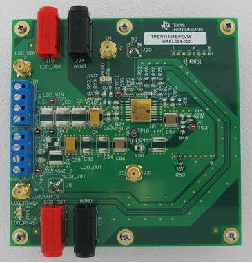
Evaluation Module Texas Instruments TPS7H1101SPEVM
The TPS7H1101-SP is a Ultra Low Dropout (LDO) linear regulator that uses a PMOS pass element configuration.
Detailed Description
The techniques employed allow for very low dropout. With an improved circuitry the TPS7H1101 operates under wide range of input voltage, from 1.5 V to 7 V which enables 6-V IN to 5-V OUT or 1.5-V IN to 1.2-V OUT voltage conversions for typical applications, while offering excellent PSRR.
The TPS7H1101 is ideally suited for high reliability applications. It features a very precise and programmable fold back current limit implementation with a very wide adjustment range.To support complex requirements of FPGAs or DSPs, the TPS7H1101 provides programmable SoftStart and PowerGood output for easy power sequencing.
TPS7H1101 is available in a 16-pin ceramic flatpack package (HKR). An Application schematic is highlighted in Figure 1 below.
A number of features are incorporated in the design to provide high reliability and system flexibility. Current foldback, overload and thermal protection are incorporated in the design to make it viable for harsh environments.TPS7H1101SPEVM also incorporates current limit protection, as well as current foldback. A resistor connected from Programmable Current limit (PCL) pin to ground sets the current limit activation point. When current limit set point is reached, it results in LDO going in current foldback mode. Output current is reduced to approximately 50% of the current limit set point.
TPS7H1101 incorporates thermal protection which disables the output when the junction temperature rises approximately 170°C, allowing the device to cool. When the junction temperature cools to approximately 150°C, the output circuitry is enabled. Depending on the power dissipation, thermal resistance and ambient temperature, the thermal protection may cycle on and off. Cycling limits the dissipation of the regulator, protecting it from damage as a result of overheating.
In order to provide system flexibility for demanding current needs, the LDO can be configured in parallel operation. This configuration will provide higher reliability (MTBF) for system needs due to reduced stress on the components, as the load current will be shared between the two LDOs. Alternately, it can also provide twice the output current to meet system needs.
Features
- Wide Vin Range 1.5V – 7V
-
TPS7H1101-SP Low Dropout Voltage
- 200 mV at 3 A (25°C)
- 61 mV at 1 A (25°C)
- Total Dose (TID) Tolererance = 100 kRad (Si)
- SEL, SEB and SEGR Immune to LET = 85 MeV/mg/cm2
- SET Immune (|dVOUT| < 5%) to LET = 85 MeV/mg/cm2
- SEFI Immune to LET = TBD MeV/mg/cm2
- Stable With Ceramic Output Capacitor
- ±2% Accuracy (2)
- Low Noise: (27 x VOUT) μV RMS
- PSRR: Over 55 dB at 1 kHz
- Programmable OCP ( over current protection) with current reading and foldback
- PowerGood Output
APPLICATIONS
- Ultra low Dropout LDO for Rad Tolerant Applications
- Supports Harsh Environment Applications
- RF Components VCOs, Receivers, ADCs, Amplifiers
- Clock Distribution
- Clean Analog Supply requirements
- TPS7H1101-SP Available in (–55°C to 125°C) Temperature Range
