Datasheet Texas Instruments ADS8507
| Manufacturer | Texas Instruments |
| Series | ADS8507 |
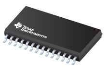
16-Bit 40KSPS Analog-to-Digital Converter w/Internal Reference and Parallel/Serial Interface
Datasheets
16-Bit 40-KSPS Low Power Sampling Analog-to-Digital Converter datasheet
PDF, 1.2 Mb, File published: Dec 19, 2006
Extract from the document
Prices
Status
| ADS8507IBDW | ADS8507IBDWG4 | ADS8507IBDWR | ADS8507IDW | ADS8507IDWG4 | ADS8507IDWR | ADS8507IDWRG4 | |
|---|---|---|---|---|---|---|---|
| Lifecycle Status | Active (Recommended for new designs) | Active (Recommended for new designs) | Active (Recommended for new designs) | Active (Recommended for new designs) | Active (Recommended for new designs) | Active (Recommended for new designs) | Active (Recommended for new designs) |
| Manufacture's Sample Availability | No | No | No | No | No | No | No |
Packaging
| ADS8507IBDW | ADS8507IBDWG4 | ADS8507IBDWR | ADS8507IDW | ADS8507IDWG4 | ADS8507IDWR | ADS8507IDWRG4 | |
|---|---|---|---|---|---|---|---|
| N | 1 | 2 | 3 | 4 | 5 | 6 | 7 |
| Pin | 28 | 28 | 28 | 28 | 28 | 28 | 28 |
| Package Type | DW | DW | DW | DW | DW | DW | DW |
| Industry STD Term | SOIC | SOIC | SOIC | SOIC | SOIC | SOIC | SOIC |
| JEDEC Code | R-PDSO-G | R-PDSO-G | R-PDSO-G | R-PDSO-G | R-PDSO-G | R-PDSO-G | R-PDSO-G |
| Package QTY | 20 | 20 | 1000 | 20 | 20 | 1000 | 1000 |
| Carrier | TUBE | TUBE | LARGE T&R | TUBE | TUBE | LARGE T&R | LARGE T&R |
| Device Marking | ADS8507I | B | ADS8507I | ADS8507I | ADS8507I | ADS8507I | ADS8507I |
| Width (mm) | 7.5 | 7.5 | 7.5 | 7.5 | 7.5 | 7.5 | 7.5 |
| Length (mm) | 17.9 | 17.9 | 17.9 | 17.9 | 17.9 | 17.9 | 17.9 |
| Thickness (mm) | 2.35 | 2.35 | 2.35 | 2.35 | 2.35 | 2.35 | 2.35 |
| Pitch (mm) | 1.27 | 1.27 | 1.27 | 1.27 | 1.27 | 1.27 | 1.27 |
| Max Height (mm) | 2.65 | 2.65 | 2.65 | 2.65 | 2.65 | 2.65 | 2.65 |
| Mechanical Data | Download | Download | Download | Download | Download | Download | Download |
Parametrics
| Parameters / Models | ADS8507IBDW | ADS8507IBDWG4 | ADS8507IBDWR | ADS8507IDW | ADS8507IDWG4 | ADS8507IDWR | ADS8507IDWRG4 |
|---|---|---|---|---|---|---|---|
| # Input Channels | 1 | 1 | 1 | 1 | 1 | 1 | 1 |
| Analog Voltage AVDD(Max), V | 5.25 | 5.25 | 5.25 | 5.25 | 5.25 | 5.25 | 5.25 |
| Analog Voltage AVDD(Min), V | 4.75 | 4.75 | 4.75 | 4.75 | 4.75 | 4.75 | 4.75 |
| Architecture | SAR | SAR | SAR | SAR | SAR | SAR | SAR |
| Digital Supply(Max), V | 5.25 | 5.25 | 5.25 | 5.25 | 5.25 | 5.25 | 5.25 |
| Digital Supply(Min), V | 4.75 | 4.75 | 4.75 | 4.75 | 4.75 | 4.75 | 4.75 |
| INL(Max), +/-LSB | 1.5 | 1.5 | 1.5 | 1.5 | 1.5 | 1.5 | 1.5 |
| Input Range(Max), V | 10 | 10 | 10 | 10 | 10 | 10 | 10 |
| Input Range(Min), V | -10 | -10 | -10 | -10 | -10 | -10 | -10 |
| Input Type | Single-Ended | Single-Ended | Single-Ended | Single-Ended | Single-Ended | Single-Ended | Single-Ended |
| Integrated Features | Daisy-Chainable,Oscillator | Daisy-Chainable,Oscillator | Daisy-Chainable,Oscillator | Daisy-Chainable,Oscillator | Daisy-Chainable,Oscillator | Daisy-Chainable,Oscillator | Daisy-Chainable,Oscillator |
| Interface | Parallel | Parallel | Parallel | Parallel | Parallel | Parallel | Parallel |
| Multi-Channel Configuration | N/A | N/A | N/A | N/A | N/A | N/A | N/A |
| Operating Temperature Range, C | -40 to 85 | -40 to 85 | -40 to 85 | -40 to 85 | -40 to 85 | -40 to 85 | -40 to 85 |
| Package Group | SOIC | SOIC | SOIC | SOIC | SOIC | SOIC | SOIC |
| Package Size: mm2:W x L, PKG | 28SOIC: 184 mm2: 10.3 x 17.9(SOIC) | 28SOIC: 184 mm2: 10.3 x 17.9(SOIC) | 28SOIC: 184 mm2: 10.3 x 17.9(SOIC) | 28SOIC: 184 mm2: 10.3 x 17.9(SOIC) | 28SOIC: 184 mm2: 10.3 x 17.9(SOIC) | 28SOIC: 184 mm2: 10.3 x 17.9(SOIC) | 28SOIC: 184 mm2: 10.3 x 17.9(SOIC) |
| Power Consumption(Typ), mW | 155 | 155 | 155 | 155 | 155 | 155 | 155 |
| Rating | Catalog | Catalog | Catalog | Catalog | Catalog | Catalog | Catalog |
| Reference Mode | Ext,Int | Ext,Int | Ext,Int | Ext,Int | Ext,Int | Ext,Int | Ext,Int |
| Resolution, Bits | 16 | 16 | 16 | 16 | 16 | 16 | 16 |
| SINAD, dB | 89.9 | 89.9 | 89.9 | 89.9 | 89.9 | 89.9 | 89.9 |
| SNR, dB | 89.9 | 89.9 | 89.9 | 89.9 | 89.9 | 89.9 | 89.9 |
| Sample Rate (max), SPS | 40kSPS | 40kSPS | 40kSPS | 40kSPS | 40kSPS | 40kSPS | 40kSPS |
| Sample Rate(Max), MSPS | 0.04 | 0.04 | 0.04 | 0.04 | 0.04 | 0.04 | 0.04 |
| THD(Typ), dB | -100 | -100 | -100 | -100 | -100 | -100 | -100 |
Eco Plan
| ADS8507IBDW | ADS8507IBDWG4 | ADS8507IBDWR | ADS8507IDW | ADS8507IDWG4 | ADS8507IDWR | ADS8507IDWRG4 | |
|---|---|---|---|---|---|---|---|
| RoHS | Compliant | Compliant | Compliant | Compliant | Compliant | Compliant | Compliant |
Application Notes
- Upgrading From ADS7806/07 To ADS8506/07 Devices (Rev. B)PDF, 88 Kb, Revision: B, File published: Nov 27, 2007
The information in this application report is for current applications using the Texas Instruments ADS7806/07 devices in a surface-mount SO-28 (DW) package. This document helps users with ADS78xx devices through potential compatibility issues when upgrading to the new ADS85xx part series. - Determining Minimum Acquisition Times for SAR ADCs, part 2PDF, 215 Kb, File published: Mar 17, 2011
The input structure circuit of a successive-approximation register analog-to-digital converter (SAR ADC) incombination with the driving circuit forms a transfer function that can be used to determine minimum acquisition times for different types of applied input signals. This application report, which builds on Determining Minimum Acquisition Times for SAR ADCs When a Step Function is Applied to
Model Line
Series: ADS8507 (7)
Manufacturer's Classification
- Semiconductors> Data Converters> Analog-to-Digital Converters (ADCs)> Precision ADCs (<=10MSPS)
