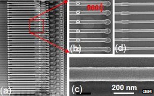
The Racetrack Circuit represents the culmination of 7 years of physics research
IBM announced that it has produced a working Racetrack Memory circuit, which could lead to chips with the capacity of hard drives, but the durability and performance of flash drives.
The new non-volatile, solid-state memory could someday replace NAND flash, which is currently at the 20 nanometer (nm) node size.

Racetrack memory uses electric currents or "spin currents" to move electrons up and down a ribbon-like nanowire that is about 240nm wide and about 20nm thick. The "spin currents" manipulate the magnetic state of nano-scale magnetic regions -- magnetic domain walls -- within the magnetic nanowires. Each nanowire represents a "cell" where electrons are stored.
IBM's chip consists of 256 Racetrack cells.

IBM tested both reads and writes on the integrated circuit, claiming I/O speeds approaching that of DRAM.
Almost all electronic equipment today is built with digital circuitry based on complementary-symmetry metal-oxide-semiconductor (CMOS) technology. As a result, IBM said it was important that its first Racetrack Memory circuit be integrated with CMOS technology on eight-inch wafers.
The company said the Racetrack Memory has far greater durability than today's NAND flash memory, which is used to make solid-state drives (SSDs) and flash cards used in cell phones and tablets. Typically, consumer-class NAND flash can sustain about 4,000 erase-write cycles, while flash devices used in large corporate data centers can sustain 50,000 to 100,000 write cycles. An IBM spokesperson claimed Racetrack Memory can sustain unlimited writes, because "it's modifying a magnetic domain" unlike NAND flash, where writes are moving charges that can ultimately degrade the material.
IBM said its memory "breakthrough" could lead to a new type of data-centric computing that allows massive amounts of stored information to be accessed in less than a billionth of a second.
The development of alternative non-volatile memories is key because some have speculated that further NAND flash development is limited because the cell walls separating where bits of data are stored in silicon are becoming too thin. As the walls thin out, the electrons that create bits of information in the cells are prone to leaking through to other cells creating data errors, which in turn requires more and more sophisticated error correction code.
