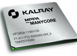
KALRAY SA, announced the availability of first samples of the 28 nanometer (nm) MPPA 256 processor targeting embedded applications among them Imaging and signal processing. This resulted from the 28nm development and production partnership established with Guc and TSMC.
First products to be ramped in volume will be processors for signal processing in an imaging application. Product qualification is scheduled for completion in Nov 2012.

Created in 2008, KALRAY is a fabless semiconductor and software company that develops, markets & sells a new generation of manycore processors for Imaging, Telecommunication infrastructures, Data Security & Network Appliances embedded applications.
KALRAY ’s technology is called MPPA for Multi-Purpose Processor Array and has solved the major two challenges of multi-core processing: the energy efficiency as well as the software scalability.
Led by Joël Monnier, former vice president of STMicroelectronics, KALRAY employs 55 engineers and is backed by French investment funds, local funds, private investors, and OSEO, a French public-sector institution who finance innovative projects brought by SME’s.
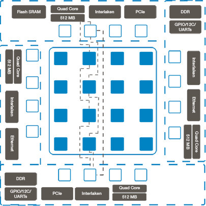
The first MPPA 256 processor integrates 256 processors onto a single silicon chip through a high bandwidth Network on Chip. The 256 processors work in parallel and communicate together via a network-on-chip just as large clusters of computers do on the Internet. The MPPA 256 is organized as 16 clusters of 16 processors and multiple MPPA chips can be interconnected at the PCB level through Interlaken interfaces to increase the processor array size and performance capability.

MPPA 256 is manufactured in 28 nm technology by world-class foundry TSMC with the lowest power consumption and highest cost efficiency. Under the TSMC VCA program, GUC provided design support as well as logistical support and manufacturing interface for KALRAY. A key reason for the unmatched efficiency of the MPPA 256 device comes from early access to TSMC’s leading-edge 28nm High Performance process.
Along with the MPPA processor family, KALRAY provides customers with its software development environment MPPA ACCESSCORE as well as development boards integrating in MPPA DEVELOPER. It offers standard GNU C/C++ development tools and libraries including primitives for task parallelism and data parallelism. The development environment also supports automatic mapping on MPPA hardware and memory resource sizing to assist developers in obtaining optimal performance.
The MPPA ACCESSCORE development environment provides a C-based programming model, which speeds up application development and debug. Several programming levels are provided for different user profiles, from Linux support for legacy functions, to a unique high level dataflow environment. Standard GCC & GDB technologies are used for compilation & debug. The KALRAY processor cores implement a proprietary VLIW architecture with advanced low-power design techniques, and integrate a high-performance IEEE 754 floating-point unit.
Features
256 VLIW cores per chip, organized in 16 clusters of 16 cores, interconnected by a high bandwidth Network-on-Chip:
- FPU 32 bits / 64 bits IEEE 754
- Virtually unlimited array extension by clustering several chips
- Standard I/Os and interfaces
- Hi-throughput memory controllers Flash / DDR, for external storage of up to 128 GB
- 28 nm CMOS technology
- Low power dissipation typ. 5 W
- Standard BGA package
Interfaces
MPPA MANYCORE processors also integrate several standard high speed I/O interfaces for simple board & system integration :
- Two 64-bit DDR3 memory controllers for high bandwidth main memory transfers
- Two 40 Gb/s (or up to eight 10 Gb/s) Ethernet controllers for efficient network processing applications
- Two 8-lane PCI Express Gen 3 interfaces for high speed connection to host or system integration
- General purpose serial and parallel I/O for standard multimedia stream exchange
- Four 4 to 8-lane high speed Interlaken interfaces for multi-MPPA MANYCORE chip system integration or connection to external FPGAs.
