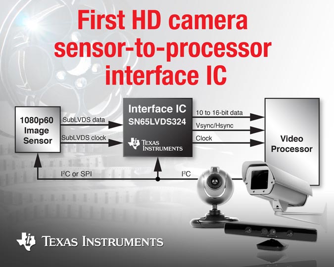
1080p60 sensor-to-processor IC reduces video system size and power consumption
Texas Instruments introduced the industry's first image sensor receiver IC to serve as a dedicated LVDS bridge between image sensors and processors. Compared to existing FPGA-based solutions, the SN65LVDS324 lowers the bill-of-materials (BOM) by 20 percent, reduces system power consumption by more than 10 percent and shrinks package size by 50 percent. It provides full HD, 1080p60 image quality in a host of video capture applications, including surveillance IP cameras and video conferencing systems, as well as industrial, consumer and professional video recording equipment.

Key features and benefits of the SN65LVDS324
- Optimized solution for sensor-to-processor interface: As a dedicated bridge for video streams between HD image sensors and processors, the SN65LVDS324 lowers BOM costs by up to 20 percent compared to existing FPGA-based solutions.
- Dedicated sensor-to-processor interface: In 1080p60 system implementations, the SN65LVDS324 typically consumes less than 150 mW, reducing system power consumption by more than 10 percent versus current FPGA solutions.
- Smallest package size: Dedicated function provides a 50-percent smaller package than current FPGAs.
- Excellent video resolution: Supports a wide range of resolutions and frame rates, up to 1080p60-full-HD to maximize system performance.
The SN65LVDS324 is an extension of TI's popular FlatLink™ and FlatLink™3G serial interface technology, which reduces the number of signal lines used for synchronous parallel data bus structures with no loss in data throughput. It is also optimized to work with a variety of processors, including TI's OMAP™ and DaVinci™ processors for video applications.
Availability, packaging and pricing
The SN65LVDS324 is available in a 4.5-mm by 7-mm, 59-ball PBGA (ZQL) package. Suggested retail pricing in 1000-unit quantities is US$2.65.
