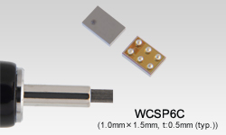
The TCK111G and TCK112G are ultra-small load switch ICs featuring low voltage operation, ultra-low ON resistance, low quiescent current, and with reverse current blocking and thermal shutdown functions.

Toshiba realizes wide input voltage operation of 1.1 V to 5.5 V and ultra-low ON resistance of 8.5 mΩ (Typ.) in 0.5 mm pitch WCSP6C (1.0 mm×1.5 mm, t: 0.5 mm (Typ.)) ultra-small package, by adopting newly developed fine CMOS processes and unique circuit technology. As additional functions, an inrush current suppressing slew rate control driver is commonly built in, and an output auto-discharge function is offered optionally. These load switch ICs are most suitable for applications that require high density mounting, such as mobile devices.
Features
- Wide input voltage operation (VIN=1.1 V to 5.5 V)
- Ultra-low ON resistance
- RON= 8.5 mΩ (Typ.) @VIN = 1.1 V, IOUT = –1.5 A
- RON= 8.4 mΩ (Typ.) @VIN = 1.8 V, IOUT = –1.5 A
- RON = 8.3 mΩ (Typ.) @VIN = 5.0 V, IOUT = –1.5 A
- Inrush current is limited by the slew rate control driver
- Reverse current blocking
- Thermal Shutdown function
- Built in Auto-discharge (TCK112G)
- Ultra-small package WCSP6C (1.0 mm × 1.5 mm, t: 0.5 mm (Typ.))
Applications
- Smart phones, tablet PCs, portable audio players, digital cameras, digital camcorders, games and other small mobile devices