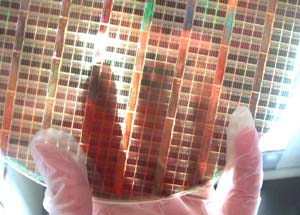
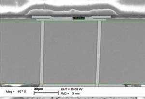
IBM today announced a breakthrough chip-stacking technology in a manufacturing environment that paves the way for three-dimensional chips that will extend Moore's Law beyond its expected limits. The technology – called "through-silicon vias" -- allows different chip components to be packaged much closer together for faster, smaller, and lower-power systems.

- 3-D for wireless communications technology: IBM is using through-silicon via technology to improve power efficiency in silicon-germanium based wireless products up to 40 percent, which leads to longer battery life. The through-silicon via technology replaces the wire bonds that are less efficient at transferring signals off of the chip.
- Power Processors explore 3-D for power grid stability: As we increase the number of processor cores on chips, one of the limitations in performance is uniform power delivery to all parts of the chip. This technique puts the power closer to the cores and allows each core to have ample access to that power, increasing processor speed while reducing power consumption up to 20 percent.
- Bringing 3-D stacking to Blue Gene supercomputing and memory arrays: The most advanced version of 3-D chip stacking will allow high-performance chips to be stacked on top of each other, for example processor-on-processor or memory-on-processor. IBM is developing this advanced technology by converting the chip that currently powers the fastest computer in the world, the IBM Blue Gene supercomputer, into a 3-D stacked chip. IBM is also using 3-D technology to fundamentally change the way memory communicates with a microprocessor, by significantly enhancing the data flow between microprocessor and memory. This capability will enable a new generation of supercomputers. A prototype SRAM design using 3-D stacking technology is being fabricated in IBM's 300 mm production line using 65 nm- node technology.
3-D chip research at IBM
IBM has been researching 3-D stacking technology for more than a decade at the IBM T.J. Watson Research Center and now at its labs around the world. The Defense Advanced Research Projects Agency (DARPA) has supported IBM in the development of tools and techniques for extending chips to the third dimension, with the aim of driving better performance and new applications of chip technologies.
IBM chip breakthroughs
This is the fifth major chip breakthrough in five months from IBM, as it leads the industry in its quest for new materials and architectures to extend Moore’s Law.
In December, IBM announced the first 45nm chips using immersion lithography and ultra-low-K interconnect dielectrics.
In January, IBM announced “high-k metal gate,” which substitutes a new material into a critical portion of the transistor that controls its primary on/off switching function. The material provides superior electrical properties, while allowing the size of the transistor to be shrunk beyond limits being reached today.
In February, IBM revealed a first-of-its-kind, on-chip memory technology that features the fastest access times ever recorded in eDRAM (embedded dynamic random access memory).
Then in March, IBM unveiled a prototype optical transceiver chipset capable of reaching speeds at least eight-times faster than optical components available today.
The IBM breakthrough enables the move from horizontal 2-D chip layouts to 3-D chip stacking, which takes chips and memory devices that traditionally sit side by side on a silicon wafer and stacks them together on top of one another. The result is a compact sandwich of components that dramatically reduces the size of the overall chip package and boosts the speed at which data flows among the functions on the chip.

The new IBM method eliminates the need for long-metal wires that connect today's 2-D chips together, instead relying on through-silicon vias, which are essentially vertical connections etched through the silicon wafer and filled with metal. These vias allow multiple chips to be stacked together, allowing greater amounts of information to be passed between the chips.
The technique shortens the distance information on a chip needs to travel by 1000 times, and allows for the addition of up to 100 times more channels, or pathways, for that information to flow compared to 2-D chips.
IBM is already running chips using the through-silicon via technology in its manufacturing line and will begin making sample chips using this method available to customers in the second half of 2007, with production in 2008. The first application of this through-silicon via technology will be in wireless communications chips that will go into power amplifiers for wireless LAN and cellular applications. 3-D technology will also be applied to a wide range of chips, including those running now in IBM’s high-performance server and supercomputing chips that power the world’s business, government and scientific efforts.
In particular, IBM is applying the new through-silicon-via technique in wireless communications chips, Power processors, Blue Gene supercomputer chips, and in high-bandwidth memory applications:
