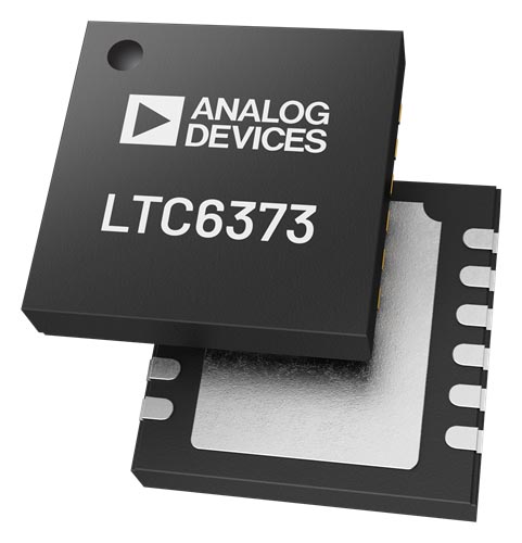
Analog Devices announced precision instrumentation amplifier LTC®6373 with fully differential outputs which includes a closely-matched internal resistor network to achieve excellent CMRR, offset voltage, gain error, gain drift, and gain nonlinearity. The user can easily program the gain to one of seven available settings through a 3-bit parallel interface (A2 to A0). The 8th state puts the part in shutdown which reduces the current consumption to 220 μA. Unlike a conventional voltage feedback amplifier, the LTC6373 maintains nearly the same bandwidth across all its gain settings.

The LTC6373 features fully differential outputs to drive high performance, differential-input ADCs. The output common mode voltage is independently adjustable via the VOCM pin. The combination of high impedance inputs, DC precision, low noise, low distortion, and high-speed differential ADC drive makes the LTC6373 an ideal candidate for optimizing data acquisition systems.
The LTC6373 is available in a 12-lead 4 mm × 4 mm DFN (LFCSP) package and is fully specified over the −40 °C to 125 °C temperature range.
Features
- Pin-Programmable Gains: G = 0.25, 0.5, 1, 2, 4, 8, 16 V/V + Shutdown
- Fully Differential Outputs
- Gain Error: 0.012% (Max)
- Gain Error Drift: 1 ppm/°C (Max)
- CMRR: 103 dB (Min), G = 16
- Input Bias Current: 25 pA (Max)
- Input Offset Voltage: 92 μV (Max), G = 16
- Input Offset Voltage Drift: 1.7 μV/°C (Max), G = 16
- –3 dB Bandwidth: 4 MHz, G = 16
- Input Noise Density: 8 nV/√Hz, G = 16
- Slew Rate: 12 V/μs, G = 16
- Adjustable Output Common Mode Voltage
- Quiescent Supply Current: 4.4 mA
- Supply Voltage Range: ±4.5 V to ±18 V
- –40 °C to 125 °C Specified Temperature Range
- Small 12-Lead 4 mm × 4 mm DFN (LFCSP) Package
Applications
- Data Acquisition Systems
- Biomedical Instrumentation
- Test and Measurement Equipment
- Differential ADC Drivers
- Single-Ended-to-Differential Conversion
- Multiplexed Applications