Diodes Incorporated introduced 2.0 A single channel load switchThe AP22916 is a small, low leakage, single P-channel power MOSFET designed for low-power consumption, load-switching applications. The power MOSFET has a typical RDS(ON) of 60 mΩ at 5 V, allowing increased load current handling capacity with a low forward voltage drop. Multiple voltages correspond to different time options to support various system load conditions.

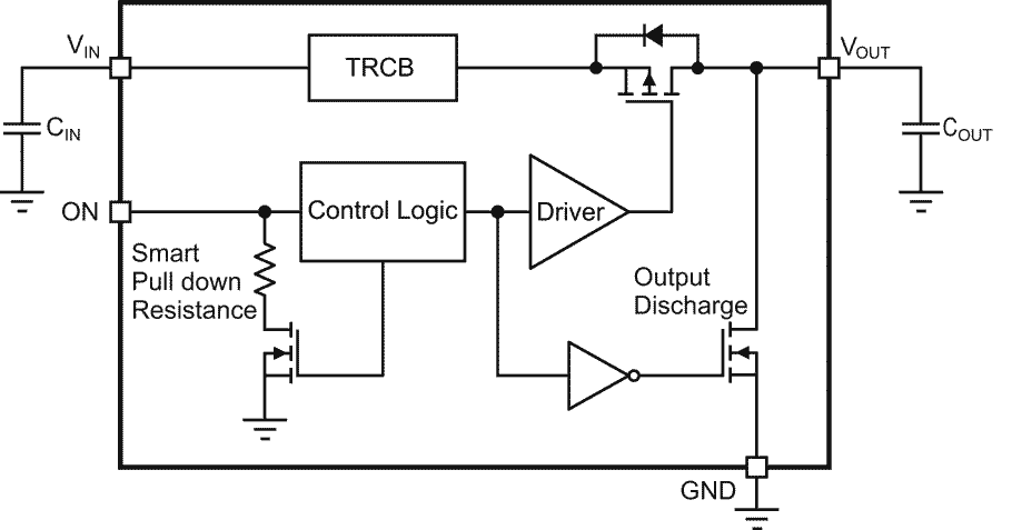
The trigger of the load switch ON pin can be controlled to be enabled or disabled by an external low voltage digital signal for sequence control application. Smart pull down feature is built in the ON pin. Once the enable voltage is higher than VIH, it will disconnect to avoid power loss. VIN and VOUT are isolated during OFF state with the TRCB (Truly Reverse Current Blocking) feature.
The AP22916 load switch is designed to operate from 1.3 V to 5.5 V, making it ideal for 1.3 V, 1.8 V, 2.5 V, 3.6 V, and 5 V systems. The typical quiescent supply current is only 0.5 µA.
The AP22916 is available in the wafer level chip scale 4-pin, X1-WLB0808-4 0.78 mm × 0.78 mm × 0.455 mm, 0.4 mm pitch package. The device is characterized for operation over a temperature range of –40 °C to +85 °C.
 |
| The AP22916 Functional Block Diagram. |
Applications
- Mobile Devices and Smart Phones
- Portable Media Devices
- Wearable Devices
- Advanced Notebook, UMPC, and MID
- Portable Medical Devices
- GPS and Navigation Equipment
