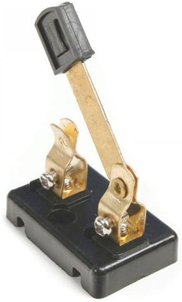
The single-pole, single-throw (SPST) switch has been a necessity since the earliest days of electricity and with good reason: It has many simply described yet vital roles in circuits spanning DC up into the highest ends of electromagnetic spectrum. While the classic knife switch provides a well-defined function and is still widely available and in use (Fig. 1), it clearly is inadequate to meet the needs today’s wired gigahertz-plus circuits due to its large size, modest bandwidth, and very slow switching speed.
 |
|
| Figure 1. | The venerable SPST knife switch has been used since the earliest days of electricity and is still useful and available, but it’s totally unsuitable for modern gigahertz functions. |
While mechanical switches can operate into the tens of gigahertz with impressive specifications – they’re marvels of electromechanical and RF design – the strong trend is toward solid-state switches. This is especially the case when signal power levels are low to moderate due to their reliability, size, switching speed, and design-in compatibility, as long as they have the needed bandwidth, of course.
ADI’s new gigahertz-class analog-RF switches
Echoing that trend is a recently introduced trio of similar silicon-based, gigahertz-class, non-reflective analog-RF switches from Analog Devices: the ADRF5010 (100 MHz to 55 GHz); ADRF5030 (100 MHz to 20 GHz); and ADRF5031 (9 kHz to 20 GHz).
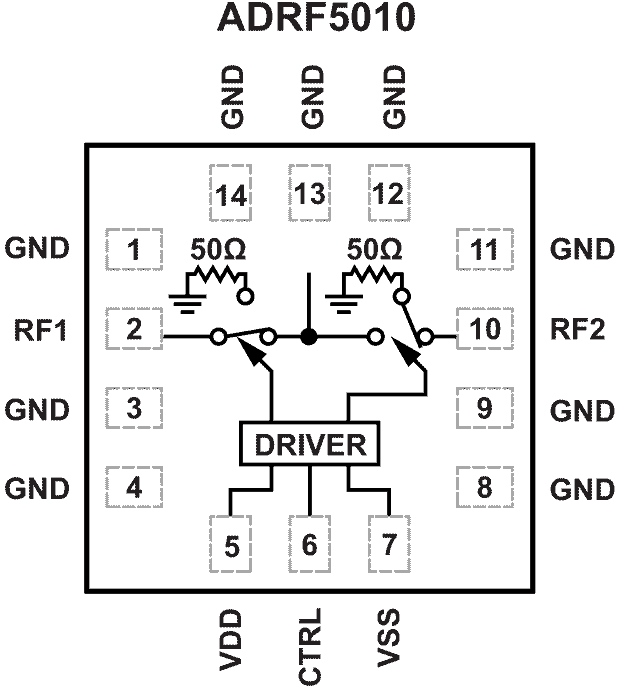
For the ADRF5010, the highest-bandwidth device in the trio (Fig. 2), target applications are the expected areas of test and instrumentation; cellular infrastructure including 5G/mmWave installations; military radios, radars, and electronic countermeasures (ECM); microwave radios and very small aperture terminals (VSATs); and industrial scanners.
 |
|
| Figure 2. | The ADRF5010 block diagram shows the functional simplicity, which can obscure the RF challenges in devising and fabricating a switch with this bandwidth and performance. |
The ADRF5010 operates from 0.1 to 55 GHz with insertion loss less than 2 dB and isolation greater 28 dB. Through internal drivers, it features CMOS- and LVTTL-compatible control with RF switching time of 30 ns, while RF settling time is 50 ns to 0.1 dB of final RF output. Input linearity is better than 33 dBm typical (P0.1 dB) and input IP3 is greater than 60 dBm (typical).
How the ADRF5010 switch handles power
Power handling is often an issue with solid-state switches. For the ADRF5010, it’s characterized for the three modes of through-path, terminated path, and hot switching, under the three conditions of peak power, pulse, and continuous (CW) power for each. For through-path, the corresponding power ratings are 36, 33, and 30 dBm; for both the terminated and CW paths, they are 33, 33, and 30 dBm, all respectively.
The ADRF5010 requires dual supply voltages of ±3.3 V and can operate with a single positive supply voltage (VDD) while the negative supply voltage (VSS) is tied to ground. In this operating condition, the small-signal performance is maintained, and the switching characteristics, linearity, and power-handling performance are derated.
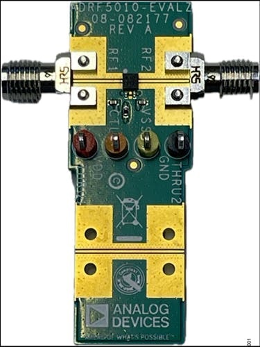
The ADRF5010 comes in a 14-lead, 2.25- × 2.25 mm, land-grid-array (LGA) package and can operate from −40 to +105 °C. Even a basic function such as a switch with its simple I/O, but operating at these frequencies, needs support beyond its datasheet. The EVAL-ADRF5010 Evaluation Board fulfills this critical role (Fig. 3). The board package includes a detailed User Guide defining test setup, PCB layout, schematic, bill of materials (BOM), and more.
 |
|
| Figure 3. | The EVAL-ADRF5010 Evaluation Board for the ADRF5010 is simple with respect to the BOM, yet also embodies the critical layout aspects for a 50-GHz part. |
Despite the apparent similarities among the three switches, they don’t share a unified datasheet. Instead, each gets its own attention via an individual landing page. Each of the landing pages calls out links to respective datasheet, evaluation board, user guide, and more.
