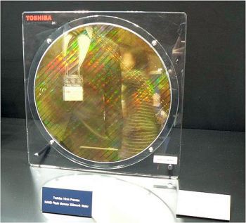
Toshiba exhibited a 300mm wafer that had 128-Gbit NAND flash memory chips and was made by using 19nm process technology at nano tech 2013. The company employed the 19nm process technology, which is the industry's most advanced process used for volume production, as well as a 3bit/cell multiple-level cell (MLC) technology.
 |
| The 300mm wafer exhibited by Toshiba |
For the 19nm process technology, Toshiba used a structure that separates floating gates with air gaps to reduce the interference between memory cells. As a result, the company ensured an operation reliability equivalent to that of 24nm process, it said. The company plans to continue to make floating-gate NAND flash memories for several more process generations by using its air-gap technology, etc.
Because the exhibited 128-Gbit NAND flash chip uses the 3bit/cell MLC technology, it can be rewritten several hundreds of times, which is about 1/10, compared with a chip using a 2bit/cell MLC technology. Therefore, the chip can be applied only to USB drives, memory cards, etc.
Toshiba focuses its resources not only on advanced process technologies and MLC technologies but also on the reduction of package thickness by stacking NAND chips in several layers. For example, it realized a slim package for 128-Gbyte memory by staking 16 layers of 30μm-thick 64-Gbit chips with a wire bonding technology.
