New Samsung DRAM Solution Signals TSV Technology is heading for Mainstream High-Capacity Memory Applications
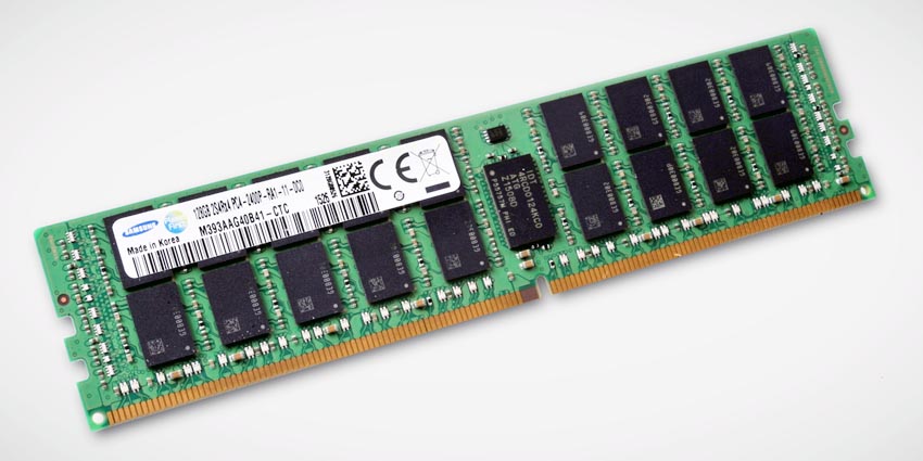
Samsung Electronics announced that it is mass producing the industry’s first “through silicon via” (TSV) double data rate-4 (DDR4) memory in 128-gigabyte (GB) modules, for enterprise servers and data centers.

Following Samsung’s introduction of the world-first 3D TSV DDR4 DRAM (64 GB) in 2014, the company’s new TSV registered dual inline memory module (RDIMM) marks another breakthrough that opens the door for ultra-high capacity memory at the enterprise level. Samsung’s new TSV DRAM module boasts the largest capacity and the highest energy efficiency of any DRAM modules today, while operating at high speed and demonstrating excellent reliability.
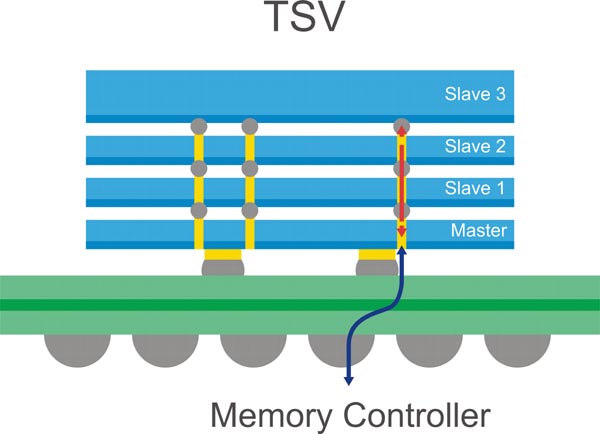
The 128 GB TSV DDR4 RDIMM is comprised of a total of 144 DDR4 chips, arranged into 36 4GB DRAM packages, each containing four 20-nanometer (nm)-based 8-gigabit (Gb) chips assembled with cutting-edge TSV packaging technology.
 |
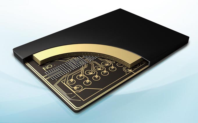
| Samsung Memory 3DS TSV DRAM Package. |
Conventional chip packages interconnect die stacks using wire bonding, whereas in TSV packages, the chip dies are ground down to a few dozen micrometers, pierced with hundreds of fine holes and vertically connected by electrodes passing through the holes, allowing for a significant boost in signal transmission. In addition to capitalizing on the industry’s highest capacity and TSV’s advanced circuitry, Samsung’s 128 GB TSV DDR4 module has a special design through which the master chip of each 4 GB package embeds the data buffer function to optimize module performance and power consumption.
As a result, Samsung’s advanced 128 GB TSV DDR4 RDIMM provides a low-power solution for next-generation servers with speeds at up to 2,400 megabits per second (Mbps), achieving nearly twice the performance, while cutting power usage by 50 percent, compared to using the previous highest capacity DRAM modules – 64 GB LRDIMMs, whose four-chip package stacks are hampered by power and speed limitations caused by their use of conventional wire bonding.
Samsung is responding to growing demand for ultra-high capacity DRAM by accelerating production of TSV technology in the market and quickly ramping up 20 nm 8 Gb DRAM chips to improve manufacturing productivity. In solidifying its technology leadership and expanding the market for premium memory solutions, the company plans to provide a complete lineup of its new high-performance TSV DRAM modules within the next several weeks including 128 GB load reduced DIMMs (LRDIMMs).

In addition, Samsung will continue to maintain its technology leadership by introducing TSV DRAM with higher performance. These will include modules with data transfer speeds of up to 2,667 Mbps and 3,200 Mbps that help to meet intensifying enterprise server needs, while expanding TSV applications into high bandwidth memory (HBM) and consumer products.

