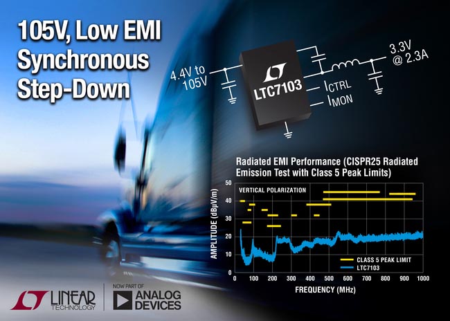
Analog Devices, Inc., which recently acquired Linear Technology Corporation, announces the LTC7103, a 2.3 A, 105 V input capable synchronous step-down switching regulator. Its wide 4.4 V to 105 V input voltage range is designed for operation from a continuously high voltage input source or from an input that has high voltage surges, eliminating the need for external surge suppression devices. This makes the LTC7103 ideal for a variety of transportation, industrial and communications applications such as 48 V automotive, 36 V to 72 V telecom, avionics and dual battery vehicle systems.

The LTC7103’s high efficiency internal power switches can deliver up to 2.3 A of continuous output current. The LTC7103 incorporates proprietary technology that reduces EMI/EMC emissions to an ultralow level, easily passing automotive CISPR#25, Class 5 limits without sacrificing efficiency. The LTC7103 delivers efficiencies over 96% while regulating a 12 V output and over 90% while regulating a 3.3 V output. To avoid noise-sensitive frequency bands, the switching frequency can be set between 200 kHz and 2 MHz, or synchronized anywhere in this range using the LTC7103’s internal phase-locked loop.
 |
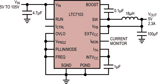
| 5 V to 105 V Input to 5 V/2.3 A Output Step-Down Regulator. |
The LTC7103 uses a unique constant frequency average current mode control architecture. This enables a fast transient response with excellent loop stability as well as fast and accurate output current programming and monitoring with no external sense resistor. This adjustable, brick-wall style current limit feature makes the LTC7103 well suited for current source applications such as battery or capacitor charging and LED lighting.
 |
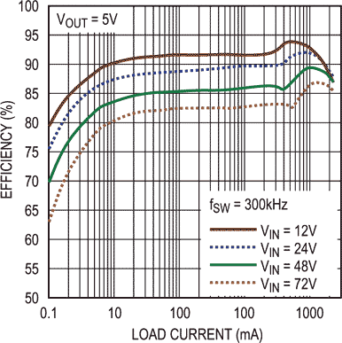
| Efficiency vs Load Current. |
The LTC7103 draws only 2 μA of input quiescent current while regulating the output voltage at no load, extending battery operating life in always-on applications. Low ripple Burst Mode® operation maintains high efficiency at light load currents while keeping output ripple small. To further minimize ripple, a pulse-skipping mode can also be selected. The LTC7103 features a low minimum on-time of 40 ns and a maximum duty cycle of 100%, enabling the output voltage to be set anywhere from 1 V up to the input voltage. The LTC7103 features eight pin-selectable fixed output voltage set points that include commonly used rails from 1.2 V to 15 V. These pre-programmed output voltages save board space and reduce the no-load quiescent current by eliminating an external resistor divider. Internal voltage loop compensation automatically adjusts based on the switching frequency to ensure both speed and stability.
 |
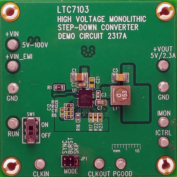
| DC2317A – 105 V, 2.3 A Low EMI Synchronous Step-Down Regulator Demo Board. |
Alternatively, the voltage loop can be optimized externally using OPTI-LOOP® compensation. The LTC7103 is packaged in a thermally enhanced 5 mm × 6 mm QFN-36(26) package with high voltage pin spacing. An industrial temperature version, the LTC7103IUHE, is tested and guaranteed to operate from a –40 °C to 125 °C operating junction temperature. Similarly a high temperature version, the LTC7103HUHE, operates from a –40 °C to 150 °C operating junction temperature. Finally, a high reliability version, the LTC7103MPUHE, operates from a –55 °C to 150 °C operating junction temperature. Pricing starts at $4.50 each in 1,000-piece quantities and all versions are available from stock.
Summary of Features: LTC7103
- Wide VIN Range: 4.4 V to 105 V (110 V Abs Max)
- Ultralow EMI/EMC Emissions: CISPR#25 Class 5 Compliant
- 2 μA IQ When Regulating 48 VIN to 3.3 VOUT
- Fast and Accurate Output Current Programming & Monitoring with No External RSENSE
- Brick Wall Current Limit
- Low Minimum On-Time: 40 ns
- Wide VOUT Range: 1 V to VIN
- 100% Maximum Duty Cycle Operation
- Programmable Fixed Frequency: 200 kHz to 2 MHz
- Eight, Pin-Selectable Fixed (1.2 V to 15 V) or Adjustable Output Voltages
- Selectable Pulse-Skipping or Low Ripple Burst Mode® Operation at Light Loads
- PLL Synchronization to External Clock
- EXTVCC LDO Powers Chip from VOUT = 3.3 V to 40 V
- OPTI-LOOP® or Fixed Internal Compensation
- Input & Output Overvoltage Protection
- Thermally Enhanced (5 mm × 6 mm) QFN Package
